Download
1 / 35
590 likes | 1.03k Views
Electronic Devices and Circuit Theory. Boylestad. Semiconductor Diodes. Chapter 1. Ch.1 Summary. Diodes. The diode is a 2-terminal device. A diode ideally conducts in only one direction. Ch.1 Summary. Diode Characteristics. Non-Conduction Region. Conduction Region.

E N D
Electronic Devices and Circuit Theory Boylestad Semiconductor Diodes Chapter 1
Ch.1 Summary Diodes The diode is a 2-terminal device. A diode ideally conducts in only one direction.
Ch.1 Summary Diode Characteristics Non-Conduction Region Conduction Region The voltage across the diode is 0 V The current is infinite The forward resistance is defined as RF = VF / IF The diode acts like a short All of the voltage is across the diode The current is 0 A The reverse resistance is defined as RR = VR / IR The diode acts like open
Ch.1 Summary Semiconductor Materials Materials commonly used in the development of semiconductor devices: Silicon (Si) Germanium (Ge) Gallium Arsenide (GaAs)
Ch.1 Summary Doping The electrical characteristics of silicon and germanium are improved by adding materials in a process called doping.There are just two types of doped semiconductor materials: n-type p-type n-type materials contain an excess of conduction band electrons. p-type materials contain an excess of valence band holes.
Ch.1 Summary p-n Junctions One end of a silicon or germanium crystal can be doped as a p-type material and the other end as an n-type material. The result is a p-n junction
Ch.1 Summary p-n Junctions At the p-n junction, the excess conduction-band electrons on the n-type side are attracted to the valence-band holes on the p-type side. The electrons in the n-type material migrate across the junction to the p-type material (electron flow). Electron migration results in anegativecharge on the p-type side of the junction and apositivecharge on the n-type side of the junction. The result is the formation of a depletion region around the junction.
Ch.1 Summary Diode Operating Conditions A diode has three operating conditions: No bias Reverse bias Forward bias
Ch.1 Summary Diode Operating Conditions No Bias No external voltage is applied: VD = 0 V There is no diode current: ID = 0 A Only a modest depletion region exists
Ch.1 Summary Diode Operating Conditions Reverse Bias External voltage is applied across the p-n junction in the opposite polarity of the p- and n-type materials.
Ch.1 Summary Diode Operating Conditions Reverse Bias The reverse voltage causes the depletion region to widen. The electrons in the n-type material are attracted toward the positive terminal of the voltage source. The holes in the p-type material are attracted toward the negative terminal of the voltage source.
Ch.1 Summary Diode Operating Conditions Forward Bias External voltage is applied across the p-n junction in the same polarity as the p- and n-type materials.
Ch.1 Summary Diode Operating Conditions Forward Bias The forward voltage causes the depletion region to narrow. The electrons and holes are pushed toward the p-n junction. The electrons and holes have sufficient energy to cross the p-n junction.
Ch.1 Summary Actual Diode Characteristics Note the regions for no bias, reverse bias, and forward bias conditions. Carefully note the scale for each of these conditions.
Ch.1 Summary Majority and Minority Carriers Two currents through a diode: Majority Carriers The majority carriers inn-typematerials are electrons. The majority carriers in p-type materials are holes. Minority Carriers The minority carriers in n-type materials are holes. The minority carriers inp-typematerials are electrons.
Ch.1 Summary Zener Region The Zener region is in the diode’s reverse-bias region. At some point the reverse bias voltage is so large the diode breaks down and the reverse current increases dramatically. The maximum reverse voltage that won’t take a diode into the zener region is called the peak inverse voltage or peak reverse voltage. The voltage that causes a diode to enter the zener region of operation is called the zener voltage (VZ).
Ch.1 Summary Forward Bias Voltage The point at which the diode changes from no-bias condition to forward-bias condition occurs when the electrons and holes are given sufficient energy to cross the p-n junction. This energy comes from the external voltage applied across the diode. The forward bias voltage required for a:gallium arsenide diode 1.2 V silicon diode 0.7 V germanium diode 0.3 V
Ch.1 Summary Temperature Effects As temperature increases it adds energy to the diode. It reduces the required forward bias voltage for forward-bias conduction. It increases the amount of reverse current in the reverse-bias condition. It increases maximum reverse bias avalanche voltage. Germanium diodes are more sensitive to temperature variations than silicon or gallium arsenide diodes.
Ch.1 Summary Resistance Levels Semiconductors react differently to DC and AC currents. There are three types of resistance: DC (static) resistanceAC (dynamic) resistanceAverage AC resistance
Ch.1 Summary DC (Static) Resistance For a specific applied DC voltage (VD) the diode has a specific current (ID) and a specific resistance (RD).
Ch.1 Summary AC (Dynamic) Resistance In the forward bias region: The resistance depends on the amount of current (ID) in the diode. The voltage across the diode is fairly constant (26 mV for 25C). rB ranges from a typical 0.1 for high power devices to 2 for low power, general purpose diodes. In some cases rB can be ignored. In the reverse bias region: The resistance is effectively infinite. The diode acts like an open.
Ch.1 Summary Average AC Resistance AC resistance can be calculated using the current and voltage values for two points on the diode characteristic curve.
Ch.1 Summary Diode Equivalent Circuit
Ch.1 Summary Diode Capacitance When reverse biased, the depletion layer is very large. The diode’s strong positive and negative polarities create capacitance (CT). The amount of capacitance depends on the reverse voltage applied. When forward biased,storage capacitance or diffusion capacitance (CD) exists as the diode voltage increases.
Ch.1 Summary Reverse Recovery Time (trr) Reverse recovery timeis the time required for a diode to stop conducting when switched from forward bias to reverse bias.
Ch.1 Summary Diode Specification Sheets Diode data sheets contain standard information, making cross-matching of diodes for replacement or design easier. • Forward Voltage (VF) at a specified current and temperature • Maximum forward current (IF) at a specified temperature • Reverse saturation current (IR) at a specified voltage and temperature • Reverse voltage rating, PIV or PRV or V(BR), at a specified temperature • Maximum power dissipation at a specified temperature • Capacitance levels • Reverse recovery time, trr • Operating temperature range
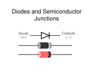
Ch.1 Summary Diode Symbol and Packaging The anode is abbreviated AThe cathode is abbreviated K
Ch.1 Summary Diode Testing Diodes are commonly tested using one of these types of equipment: Diode checker Ohmmeter Curve tracer
Ch.1 Summary Diode Checker Many digital multimeters have a diode checking function. The diode should be tested out of circuit. A normal diode exhibits its forward voltage: Gallium arsenide 1.2 V Silicon diode 0.7 V Germanium diode 0.3 V
Ch.1 Summary Ohmmeter An ohmmeter set on a low Ohms scale can be used to test a diode. The diode should be tested out of circuit.
Ch.1 Summary Curve Tracer A curve tracer displays the characteristic curve of a diode in the test circuit. This curve can be compared to the specifications of the diode from a data sheet.
Ch.1 Summary Other Types of Diodes There are several types of diodes besides the standard p-n junction diode. Three of the more common are: Zener diodes Light-emitting diodes Diode arrays
Ch.1 Summary Zener Diode A Zener diode is one that is designed to safely operate in its zener region; i.e., biased at the Zener voltage (VZ). Common zener diode voltage ratings are between 1.8 V and 200 V
Ch.1 Summary Light-Emitting Diode (LED) An LED emits light when it is forward biased, which can be in the infrared or visible spectrum. The forward bias voltage is usually in the range of 2 V to 3 V.
Ch.1 Summary Diode Arrays Common Anode Common Cathode Multiple diodes can be packaged together in an integrated circuit (IC). A variety of diode configurations are available.