Download
1 / 20
220 likes | 365 Views
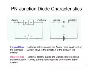
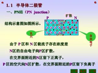
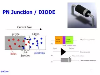
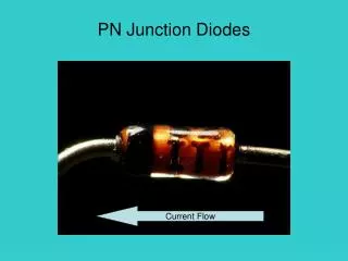
Diodes are the semiconductor pn junction devices. They are formed by creating p-type and n-type semiconductors in a single Si/ Ge (mostly) crystal. They are unidirectional devices. Every diode requires a minimum potential across it to allow a significant current to flow through it.

E N D
Diodes are the semiconductor pn junction devices. • They are formed by creating p-type and n-type semiconductors in a single Si/Ge (mostly) crystal. • They are unidirectional devices. • Every diode requires a minimum potential across it to allow a significant current to flow through it. • This voltage is called as cut-in voltage. • The VI relationship for a normal diode is exponential and is given by, Id=I0 (e (Vd/ηVt)-1)
where, Id = current flowing through diode I0 = Reverse saturation current Vd = Voltage across diode η = Material constant (actually it depends on doping level & manufacturing process also and varies between 1 to 2) • The reverse voltage at which the pn junction is damaged called as breakdown voltage (here diode may get permanently open or close) • Diode doesn’t follow its current equation in breakdown region
Photo Diode Signal Diode Gunn Diode Zener Diode Light Emitting Diode Varactor Diode/ Varicap Schottky Diode Tunnel / Esaki Diode
Transistor is a solid state device made up of Silicon or Germanium. • The name is derived from “Transfer Resistor” • There are two main types of transistors, • Bipolar Junction transistor (BJT) • NPN • PNP • Field Effect Transistor (FET) • JFET • MOSFET
These are constructed on a single Si / Ge crystal by doping 3 p-type and n-type impurities alternately. • The doping sequence can be • n-p-n • p-n-p • It has two pn junctions and 3 doped regions • Transistor can’t be constructed by adding two diodes back to back, because it will have 4 doped regions. • The three regions in transistors are • Emitter • Base • Collector
NPN transistor PNP Transistor
The three regions are called as emitter (extreme left), base (middle) and collector (extreme right) • Input can be given between any two terminals and output can be taken from any two terminals keeping one terminal common to both input and output. • Depending upon the terminal which is kept common to both i/p and o/p, it can be configured in three ways. • Common Base (CB) config. • Common Emitter (CE) config. • Common Collector (CC) config.
In this configuration, base is kept common between input and output. • Input is given between base & emitter and output is taken between base & collector. • This configuration is also known as Grounded base configuration. • The output equation can be given as, VCB = V0 = VCC – ICRL
In this configuration, collector is kept common between input and output. • The output is obtained by connecting a load resistance (RL) in emitter • This configuration is also known as emitter follower (because voltage across the emitter resistor follows the input voltage at base) or buffer • The output equation can be given as, V0 = IERL
In this configuration, emitter is kept common between input and output. • Input is given between base & emitter and output is taken between emitter & collector. • The output equation can be given as, • VCE = V0 = VCC – ICRL
Input Characteristics • This is plotted for IB Vs. VBE keeping VCE constant. • Firstly VCE is kept constant and then VBE is slowly increased and corresponding values of IB are recorded. • This is done for different values of VCE. • Output Characteristics • This is plotted for IC Vs. VCE keeping IB constant. • Firstly IB is kept constant and then VCE is slowly increased and corresponding values of IC are recorded. • This is done for different values of IB.