Download
1 / 11
110 likes | 210 Views
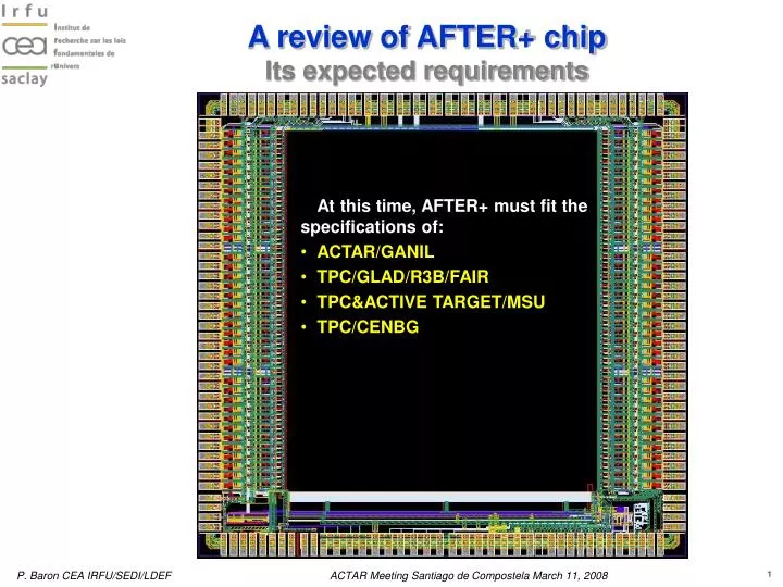
A review of AFTER+ chip Its expected requirements. At this time, AFTER+ must fit the specifications of: ACTAR/GANIL TPC/GLAD/R3B/FAIR TPC&ACTIVE TARGET/MSU TPC/CENBG. AFTER+. Σ 72 discriminator outputs. inhibit. 1 channel. DAC. BUFFER. Discri. Charge range. 76 to 1. FILTER. SCA.

E N D
A review of AFTER+ chipIts expected requirements At this time, AFTER+ must fit the specifications of: • ACTAR/GANIL • TPC/GLAD/R3B/FAIR • TPC&ACTIVE TARGET/MSU • TPC/CENBG
AFTER+ Σ 72 discriminator outputs inhibit 1 channel DAC BUFFER Discri Charge range 76 to 1 FILTER SCA ADC external 12-bit ADC [AD9229] x72in(76out) CSA ADC 511 cells tpeak BUFFER SCA MANAGER Power on Reset Readout Mode TEST Asic “Spy” Mode SLOW CONTROL W / R CK In Test Serial Interface CK CSA;CR;SCAin (N°1) Mode AFTER+: Architecture Main features for AFTER+: • 72 Analog Channels; Slow Control & test. Main features for the channel • Input Current Polarity: positive or negative. • CSA + PZC + Filter (semi-Gaussian order 2). [Possibility to bypass the CSA and to enter directly to the filter or SCA input]. • 511 analog memory cells. • Auto Triggering: discriminator + threshold (DAC) + inhibition. Main features for the readout • Analog OR of the 72 discriminator outputs [1 current output]. • Address of the hit channel (through slow control link). • 4 SCA readout modes.
inhibit DAC Discri ADC DAC AFTER+: Mode of operation Asic management (local or global) Trigger_out AFTER+ Trigger control: multiplicity & detection 1 channel Reset Reset: hit_channel register 76 to 1 x72in(76out) SCA FILTER CSA ADC control BUFFER SCA MANAGER TEST SLOW CONTROL Write Read SCA read: READ & CKread SCA write: Write & CKwrite Slow control: Din, Dout, CK, CS Test: DAC Stop Sampling:on external or local Trigger SCA_in Discri_in Channel i Discri_out Hit_channel Trigger_out Write_SCA Read_Address_hit channel Read_SCA Data_SCA_out Reset SCA write SCA read address read SCA write
AFTER+ Requirements: Charge measurement • Charge Range • 3 charge ranges • 120fC [750keV], 1pC [6.25MeV] & 10pC [62.5MeV] • Adjustable / channel • Charge Measurement • Output dynamic range: • 2V (differential); match the ADC specification [12-bit ADC AD9229] • I.N.L: < 2% • Peaking Time • 16 values: 50ns to 1µs • Adjustable / chip • Charge Resolution • Configuration: Charge Range:120fC; Peaking Time: 200ns; Cin Asic < 30pF • asked: < 600 e- rms; possibility: < 850 e- rms.
Sampling frequency • Reading frequency • 1 MHz to 100 MHz • 20 MHz to 25 MHz AFTER+ Requirements: SCA • SCA memory cells • 511 • Time Resolution • Correlated to the sampling frequency • Jitter: < 2ns
OR_hit channel Iin Iin Iin Iin I=Iin I=Iin I=Iin I=Iin 72 xIin Hit channel i Hit channel 01 Hit channel 72 Hit channel 02 Iin Slow Control Register (2 bits) AFTER+ Requirements: trigger • Discriminator solution • L.E.D • Inhibition: / channel • Trigger output • Current: Σ 72 discriminators • Trigger time resolution • The trigger time resolution will be dependent on the input charge, threshold & peaking time value => no spec.
AFTER+ Requirements: trigger • Input dynamic range • 5% of asic input dynamic range • IN.L: < 5 % • Threshold value • Common DAC: 3 bits + 1 bit of polarity • Individual DAC: 4 bits • Comment: DACLSB = 0.04% of asic input dynamic range • Minimum threshold value • Minimum value: ≥ noise • Comment: [Preliminary result] 120fC; 30pF; 200ns • minimum # 3 keV ( 0.5fC; 0.4 % of asic input dynamic range)
Readout mode: 1 channel means 511 SCA cells • All channels [Treadout # 2ms] • Hit channels [Treadout # 26µs x nchannel] • Specific channels [Treadout # 26µs x nchannel] • internal Readout buffer • 2 [controlled by slow control] • Comment: for all the 4 readout modes ?? AFTER+ Requirements: Readout • Readout frequency • 20 MHz to 25 MHz • Readout mode: 1 channel means 511, 256 or 128 SCA cells • Comment: for all the 3 readout modes ??
Calibration • External capacitor; test on 1 channel / 72 AFTER+ Requirements: Test • “test” • 3 internal capacitors (1 / charge range); test on 1 channel / 72 • Functional • 1 internal capacitor/channel; test on 1, few or all channels
Counting Rate • 1 kHz max. [CENBG] AFTER+ Requirements: Counting rate & Power • Power consumption • < 10 mW / channel
AFTER+ Requirements: Conclusion • The design of the chip could be started if all the requirements are defined, approved and fixed. • Don’t forget that this chip is only one element of the global readout electronic. • Generally, the specifications for the asic and the global electronic architecture are defined in the same time.