Download
1 / 17
320 likes | 1.17k Views
Atomic Force Microscopy (AFM). Stephen Fahey Ph.D. Advisor: Professor Sivananthan October 16, 2009. Scanning Tunneling Microscope (STM) Atomic Force Microscope (AFM) Today’s Sample. Outline. Tunneling. Charge carriers can apparently violate E conservation!.

E N D
Atomic Force Microscopy (AFM) Stephen Fahey Ph.D. Advisor: Professor Sivananthan October 16, 2009
Scanning Tunneling Microscope (STM) Atomic Force Microscope (AFM) Today’s Sample Outline
Tunneling Charge carriers can apparently violate E conservation!
Scanning Tunneling Microscope 1981 Binnig and Rohrer observe tunneling between a metal tip and a flat surface This observation led to the first STM shortly thereafter (~ 1982) • Exponential dependence of J • Piezoelectric materials • Amplifier circuitry • Low oxide tip
STM Observations (1982) Si (111) 7x7 reconstruction (1983) Nobel Prize (1986)
More STM • Scanning Tunneling Spectroscopy (STS) • Single atom manipulation • Multiple probes
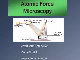
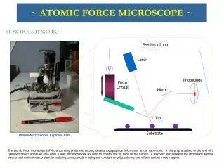
Atomic Force Microscope (AFM) • STM not good for insulators • ~ 1985 Binnig, Quate, and Gerber used STM as feedback of first AFM • AFMs can typically be operated in either tapping-mode or contact-mode
Prevalence of the Harmonic Oscillator Taylor Series and Potential Energy Inter-atomic potential Separation
Damped and Driven Harmonic Oscillator • Complementary Function ( F = 0 ), plus Particular Solution • Motion has resonance frequencies • Motion is phase shifted • Less damping increases “Q” and sharpens phase vs. frequency curve • More damping decreases resonance frequency • Resonance frequency shifts under an external applied field gradient
Tip-Sample Forces • Pauli and Coulomb repulsive • Van der Waals attractive Tip-Sample Cantilever Deflection Piezo Height
Typical AFM data Carbon Nanotubes Unidym 2 μm GaN Northwestern U. BaF2 / CaF2 / Si
Artifacts • Large scale tip shape • Tip radius • Tip side-wall angles • Double tip (or more) • Contamination of tip • Bow from Piezoelectric elements • Background noise • Feedback laser interference • Response time limited errors (t ~ 10-4 seconds)
AFM System from Veeco • Dimension 3100 • Etched Si probe tips with Al back coating • Movable sample stage with optical microscope for course positioning • Stepper motors for micrometer postioning of tip • Friendly software and feedback control circuitry
Interferrometrically Patterned Today’s Sample
Final Sample 5 μm
STM ~ 1982 led to AFM ~ 1986 Both are powerful and beautiful characterization techniques Conclusion