Download
1 / 48
480 likes | 484 Views
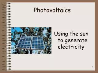
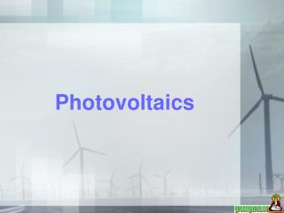
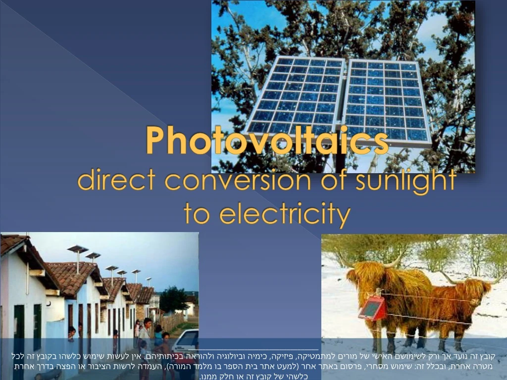
Photovoltaics direct conversion of sunlight to electricity.

E N D
Photovoltaicsdirect conversion of sunlight to electricity _____________________________________קובץ זה נועד אך ורק לשימושם האישי של מורים למתמטיקה, פיזיקה, כימיה וביולוגיה ולהוראה בכיתותיהם. אין לעשות שימוש כלשהו בקובץ זה לכל מטרה אחרת, ובכלל זה: שימוש מסחרי, פרסום באתר אחר (למעט אתר בית הספר בו מלמד המורה), העמדה לרשות הציבור או הפצה בדרך אחרת כלשהי של קובץ זה או חלק ממנו.
History of solar cells • 1839: Edmund Becquerel: photovoltaic effect • 1883: Charles Fritts: first solar cells made from selenium wafers • 1921: Albert Einstein: Nobel Prize for theories about photoelectric effect. • 1954: Bell Labs announces the invention of the first modern silicon solar cell. • 1957: Hoffman Electronics achieved 14% efficient cell. • 1964: The Nimbus spacecraft was launched with a 470-W PV array. • 1985: Solar cell more than 20% efficient.
Solar Energy Conversion Toward 1 Terawatt, 2008 , D. Ginley et al.
Semiconductors Metals Insulators Titanium Oxide Silicon Magnesium Semiconductors/ insulators Metals
Fermi Energy • The chemical potential of an electron (at absolute zero) • Only electron with energies greater than the Fermi energy may be acted on and accelerated in the present of an electric field= free electrons.
Silicon- a semiconductor In a silicon lattice, all silicon atoms bond perfectly to four neighbors, leaving no free electrons to conduct electric current. This makes a silicon crystal an insulator rather than a conductor.
p- doping n- doping You can change the behavior of silicon and turn it into a conductor by doping it. In doping, you mix a small amount of an impurity into the silicon crystal.
Built in potential P/N junc. N P
e - h+ e - h+ load The Photovoltaic (PV) effect: Light Absorption + Carrier Generation + Carrier Collection charge separation
Light Photoelectric effect P/N junc. N P
Current – Voltage diagram Power = Current Voltage V = IR C- OPV- open circuit R= ∞ A- Short circuit- R=0
Efficiency of a solar cell depends on: Light absorption↑ (band gap) Conduction↑ Recombination↓ Current Voltage
n h e e - - high energy photon - partial loss e e - - Energy h n p p - - type type useable photo- n n - - type type voltage h h + + low energy photon-total loss Energy Losses in single p-n junction solar cell
Quantum conversiona Threshold process Solar Energy Spectrum Infra- visible ultra- -Red -violet (IR) (UV)
Most solar energy is “wasted” as heat
Absorption Spectra of Some Promising PV Materials 106 105 a-SiGe:H a-Si:H CuInSe2 104 Absorption coefficient (cm-1) CdTe 103 1.82 eV Crystalline Si 102 101 1.0 1.5 2.0 2.5 Photon energy hw (eV) 026587272 Thin-Film Solar Cells, Y. Hamakawa, Springer
The ideal cell 1. No reflection anti-reflective coating 2. No recombination high quality semiconductor, thin film 3. Maximum absorbance of light band gap of 1.1-1.4eV, thick film? 4. Maximum conduction/ minimum resistance high quality of semiconductor
Quantum dot Cells (optics!) 3d generation 2nd generation 1st generation, Si next generations • 4.5 6 15 • nm Nanocrystalline TiO2 Cheaper, simpler 15-20 nm m cm Development of Solar Cells
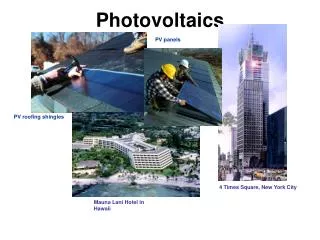
Si,Ge GaAs InP CdTe CuInSe2 Phenylene- Vinylidene ++ Ru dye-TiO2 Current types of PV devices Primarily based on solid-state electronic material systems • First genetarion: • Single or multi-crystal • Polycrystalline • Amorphous thin film • Second generation: • CdTe • CIGS • GaAs • Third generation: • Quantum dots technology • Multi-junction cell • Non-semiconductor technology- polymer cells • Thermophotonics • Nanosolar
41.1% Multi-junction 25% Crystalline Silicon Thin films- 20% CIGS 16.7% CdTe 6.4% organic SC
Crystalline Silicon 25% efficiency Wafers cost accounts for over 50% of the total module cost
TFSC- Thin Film Solar Cell • Deposition of one or more thin layers of PV material on a substrate (usually glass). • Mass production- CdTe- cadmium telluride. CIGS- copper indium gallium selenide. TFSi- thin film silicon. (Dye sensitized)
Why TFSC? • A big part of the expence is the price of the substrate - as in silicon wafer. • Thin film- reducing the width of the substrate from micron to nanometers- minor diffusion length.
TFSC- Thin Film Solar Cell- CIGS Highest efficiency tricky to deposit Cd toxic In scarce n-type p-type TCO= transparent conducting oxide 20% efficiency
TFSC- Thin Film Solar Cell- CdTe Easily deposited Cd toxic Te scarce 16.7% efficiency
What can we do? Better utilization of sunlight: Photon management
Third generation • Efficient- Infrared, UV spectrum • Light • Flexible • Compact
Multi-junction PV Thermodynamic Efficiency Limits non-concentrated Sunlight (AM 1.5)
Organic solar cells • Absorption of photons leads to the creation of bound electron-hole (excitation) pairs with a binding energy of 0.5 eV. • The excitation pairs have to diffuse to dislocation sites where their charge can be seperated and transported to the contacts. • Only about 30% of incident light is absorbed - polymers have bandgaps of above 2 eV.
Organic solar cells • Cheap!! • Less than 100nm thick • Processing performed at room temperature - can be preformed on flexible substrates, cheaper methods.
Definition of efficiency: • Highest measured cell efficiencies: • ~ 35% III-V triple junction cell • (41% IV + III-V cells, with concentration) • ~ 25% single crystalline Si • ~ 20% single junction PX thin films (CIGS, Si) • ~ 11% dye sensitized solar cells (DSSC) • ~ 6.5% organic PV