Download
1 / 25
250 likes | 496 Views
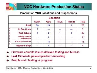
MTF7 hardware status. Alex Madorsky for UF group. Muon Trigger structure rework. Barrel TF. Overlap TF. Endcap TF. - Overlap TF is now separated from Endcap and Barrel. uTCA chassis. Sector Processor (SP) occupies 2 uTCA slots 12 units in system

E N D
MTF7 hardware status Alex Madorsky for UF group
Muon Trigger structure rework Barrel TF Overlap TF Endcap TF - Overlap TF is now separated from Endcap and Barrel
uTCA chassis • Sector Processor (SP) • occupies 2 uTCA slots • 12 units in system • All chassis use AMC13 (designed by Boston University) • Clocking, TTC, and DAQ • 3 units • Plan to control boards via PCI express • Will be compatible with IPbus as well Chassis #1 SP SP SP SP SP Chassis #2 SP SP SP SP SP Chassis #3 SP SP
MTF6 prototype • MTF6 prototype • based on Virtex-6 FPGA • Modular design • Makes future partial upgrades easier Custom backplane Optical module Core logic module Pt LUT module Custom backplane Core logic module Optical module
Optical module Optical transmitters (2 out of 3 installed) Custom backplane connector Optical receivers (2 out of 7 installed) Backplane redrivers uTCA connector MMC
Optical communication test • @3.2 Gbps • 47 input channels • Transmission from: • Loopback • Muon Port Card • Earlier VME prototype (2010) • For MPC and VME prototype clock was synchronized with VME crate • Twisted pair LVDS connection to uTCA backplane • @10 Gbps • 6 input channels • Asynchronous clock • Transmission from: • Loopback • Earlier 10Gbps prototype (2006) • Results • Zero errors for hours Eye pattern @10 Gbps. GTH receiver input.
Integration tests • Mimicking real system setup: • Sending data from 2 MPCs to MTF6 • Each MPC clocked by separate CCB • MTF6 receives clock from AMC13 • CCBs and AMC13 receive clock from common source (TTCvi) • Types of tests: • PRBS • Random data via test FIFOs • Latest MPC data format used • Result: • No errors.
PT LUT module Clock synthesis and distribution Base board connector Glue logic FPGA (Spartan-6) RLDRAM3 memory 16 chips, 8 on each side (clamshell topology) Total size: 512M x 18 bits ≈ 1GB Upgrade possible to 2 GB with bigger RLDRAM3 chips (no board redesign) DC-DC converters
PT LUT tests • Parameters: • RLDRAM clock : 200 MHz • Address & control: 200 Mbps each bit • Data: 400 Mbps each bit • RLDRAM can tolerate up to ~1GHz clock. However: • Hard to implement in FPGA • Needed for burst-oriented applications mostly • Does not change latency for random address access • Lower clk F lower power consumption • Tests performed (random data, full 1GB space): • Writing into consecutive addresses • Reading from consecutive addresses • Reading from random addresses • No errors detected • Except soldering defects in one RLDRAM chip
Base board PT LUT connector Linear regulators Core logic FPGA Switching regulators Control FPGA Clock modules
MTF7 tests • Assembled boards received January 30th • Base board • Clock modules (synchronous and asynchronous) • Custom backplane • Wisconsin MMC code adapted for MTF7 • Power sequencer reworked • Added more voltage and current sensors • 32 sensors total • Power supplies (switching and linear) tested • Support fully programmed core logic FPGA • Voltages and ripple well within specified limits • Verified using IBERT containing 80 GTH transceivers and 40% of FPGA logic • Total power consumption ~50W • Will grow to ~60W when control FPGA is fully programmed, and more logic is used in core FPGA • Still well below 80W uTCA limit
MTF7 tests • Clock module programming implemented in control FPGA • 12 Asynchronous clocks derived from 250 MHz oscillator • 10 Gbps data links • PCI express • DAQ • 12 Syncronous clocks derived from LHC clock • Slower data links (3.2 Gbps, 1.6 Gbps) • FPGA fabric clock • PCI express connection tested • Full functionality is not implemented so far • Only connection to PCIe switch verified • Next: • Test serial communication • Just started on this
Optical patch panel schematics Outputs to overlap TF Outputs to EMU TF Inputs from CSCs Outputs to neighbor overlap TF Inputs from RPCs Outputs to neighbor sector EMU TF
Optical patch panel Slack spools Splitters LC-LC adapters Fanouts MTP connectors Inputs & outputs
Conclusions • MTF7 prototype tests in progress • Optical patch panel prototype assembled but not fully tested yet
Motivations for upgrade • Current Endcap Trigger is adequate for LHC luminosities before the upgrade • The following improvements are needed for the upgrade: • Transverse Momentum (pT) assignment • Final pTassignment is currently done with 2MB LUT • Address space is already over-saturated • Need bigger pTassignment memory • Trigger primitives bandwidth • Current system selects only 3 best primitives in each sector • Reduces efficiency when multiple muons are in small region (10o) • Problematic in high-pileup conditions • Need to import all primitives on each BX • 90 per sector • Also need to import other data • Resistive Plate Chambers (RPC) • Potentially: Gas Electron Multipliers (GEM) • The above means: • Higher input bandwidth • Bigger FPGA
Block diagram Best 3 Muonsin each sector (36 total) To GMT From MPCs 60 12-corefibers, 8 cores used in each. 90 trig. primitives per 60° sector 3.2 Gbps Sector Processors 12 units 60° sector each Optical plant (fanouts and splitters) From RPC Up to 216 fibers at 1.6 Gbps (may be concentrated to higher bandwidth and fewer fibers) To Overlap Track Finder
MTF6 Core logic module Custom backplane connector PT LUT module connector Control FPGA JTAG Core logic FPGA FMM connector Control FPGA SD card connector MMC USB console uTCA connector MMC JTAG 1Gb FLASH Main FPGA firmware storage MMC CPU MMC = Module Management Controller Estimated power consumption: ~50 W (assuming FPGAs nearly full) PT LUT mezzanine not included
MTF6 Core logic module • Serial I/O: • 53 GTX receivers (up to 4.8 Gbps) • 8 GTH receivers (10 Gbps) • 12 GTX transmitters (up to 4.8 Gbps) • 2 GTH transmitters (10 Gbps) • MMC – Wisconsin design • See this link for details • Configuration memory for Core FPGA: • PC28F00AP30EFA • 1 Gb parallel FLASH • Can be used to store any other information (in addition to firmware) • Permanent configuration settings • Multiple firmware versions • SD card slot • Can also be used to store Core FPGA firmware and settings • Fast Monitoring (FMM) connector • Compatible with the current FMM system • Control interfaces: • PCI express • IPbus
Optical module • Receivers: • 7 12-channel RX • Avago’s AFBR-820BEZ • 84 RX channels • Transmitters: • 3 12-channel TX • Avago’s AFBR-810BEZ • 28 TX channels (12+12+4) • All of them 10 Gbps parts • Not enough space on front panel to accommodate all • TX parts located inside • connect with short fibers to MPO fiber couplers on front panel • Tight but enough space to fit couplers on top of AFBR-820 parts. • Receivers are on front panel to minimize count of fiber-to-fiber transitions for inputs • Control: • Wisconsin MMC design, no FPGA • Compatible with future Virtex-7 design of Core logic board
Optical components tests • Trunk cable identical to what will be used for Endcap TF • Total length (126 m) exceeds actual fiber length in Endcap TF system (113 m) • Results: • @3.2 Gbps: no errors with 2-way and 4-way spltting • @1.6 Gbps: 2-way splitting OK, errors with 4-way • Newer optical receivers lose efficiency at low bitrates Couplers MTF6 MPC or MTF6 63-meter trunk cable (2 lengths) Fanout Fanout Splitters
PCI Express tests: Setup 2012 Prototype NAT-MCH (not visible) PC adapter Fiber (up to 50 m) Motherboard AMC113 (uTCA PCIE adapter) Multiple PC adapters tested Best results: HIB35-x4 Also least expensive
PCI express performance • Results of performance tests at UF: • Sustained performance, all overheads included • 5 meter fiber: • Reading: 2.4 Gbps • Writing: 2.88 Gbps • 50 meter fiber: • Reading: 2.3 Gbps • Writing: 2.88 Gbps • Single lane PCIe gen 2 • Performance is scalable with lanes (x2, x4) • IPbus performance (for reference): • 0.29 Gbps • Tests with other type of MCH in progress • UTC002 (Vadatech) • Plan to develop uHAL interface for PCIe • Standard in CMS
More MTF6 tests • Other tests • IPbustest: OK • AMC13 clocking: OK • AMC13 DAQ and TTC: still in progress