Download
1 / 28
290 likes | 478 Views
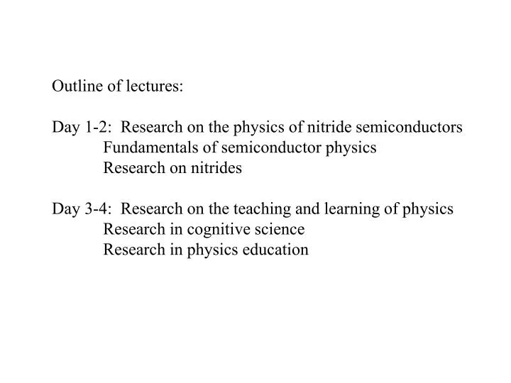
Outline of lectures: Day 1-2: Research on the physics of nitride semiconductors Fundamentals of semiconductor physics Research on nitrides Day 3-4: Research on the teaching and learning of physics Research in cognitive science Research in physics education.

E N D
Outline of lectures: Day 1-2: Research on the physics of nitride semiconductors Fundamentals of semiconductor physics Research on nitrides Day 3-4: Research on the teaching and learning of physics Research in cognitive science Research in physics education
Nitride semiconductors and their applicationsPart I: Basic Semiconductor Physics “One should not work on semiconductors, that is a filthy mess; who knows whether they really exist.” Attributed to Wolfgang Pauli (1931)
What are semiconductors? • Metals, semimetals, semiconductors, insulators • Characteristics • Conductivity increases dramatically with temperature (conductivity at T = 0 K is zero) • Conductivity changes dramatically with addition of small amounts of impurities • Applications • Anything in which you want to control the flow of current (transistors, amplifiers, microprocessors, etc.) • Devices for producing light • Radiation detectors
History of semiconductors • 1833 Michael Faraday discovers temperature-dependent conductivity of silver sulfide • 1873 Willoughby Smith discovers photoconductivity of selenium • 1874 Ferdinand Braun discovers that point contacts on some metal sulfides are rectifying • 1947 John Bardeen, Walter Brattain, and William Shockley invent the transistor
Semiconductor materials Examples: IV: C, Si, Ge III-V: GaAs, GaN, InP, AlSb, GaAlAs, GaInN II-VI: ZnSe, CdTe
Physical Structure Basic lattice Face-centered cubic (fcc) Diamond structure Si, Ge Zincblende GaAs, InP, ZnS,... About 1022 atoms in each cm3. Zincblende: ABCABC… Wurtzite: ABABAB…
Electronic Structure • Bands analogous to electronic energy levels of single atoms • Band gap between 0 and 5 eV (1 eV = 3.83 x 10⁻²³ Cal) • Electrons in valence band are involved in atomic bonding • Electrons in conduction band are free to wander the crystal • Temperature dependence of resistance is due to thermal excitation of electrons across bandgap
Band structure of Si Chelikowski and Cohen, Phys. Rev. B 14, 556 (1976)
Growth (bulk) • Czochralski growth (1918) • Crystals grown near melting point of material (> 1410 °C for silicon) • Boules up to 12” diameter and 6 feet long • Growth rate: ~few mm/min • Used for Si, Ge, GaAs, InP From http://kottan-labs.bgsu.edu/teaching/workshop2001/chapter5.htm
Growth (layers) • MOCVD (Metal-Organic Chemical Vapor Deposition) • Also known as MOVPE, etc. • Growth temperatures near melting point • Growth rate ~1 mm/min. From http://kottan-labs.bgsu.edu/teaching/workshop2001/chapter5.htm
Fun facts about AsH3 • OSHA Permissible Exposure Limit = 0.05 ppm (averaged over 8 hour work shift) • Detection: Garlic-like or fishy odor at 0.5 ppm • IDLH (Immediately Dangerous to Life or Health) at 6 ppm. (IDLH for other toxic gases such as Chlorine or Phosphine are >1000 ppm.)
Growth (layers) • MBE (Molecular-Beam Epitaxy) • Low growth temperature • Growth rate ~few mm/hr. • Can grow atomically flat surfaces and monolayers From http://kottan-labs.bgsu.edu/teaching/workshop2001/chapter5.htm
Doping • Adding impurities to alter the electrical properties • n-type (donors) or p-type (acceptors) • Deep or shallow • Single/double/triple n-type p-type
Doping • Shallow donors can be modeled as hydrogen atoms in a dielectric medium. • The donor electron level is only a few (6-50) meV below conduction band. • Hydrogen-like and helium-like levels are observed.
Doping • Grown in • Diffusion • Neutron transmutation(30Si(n,g)31Si --> 31P + b-, T1/2=2.6 hr.) • Ion implantation
Characterization (electrical) Hall effect enables determination of: • charge of carriers • density of carriers • binding energy of carriers (temperature dependent)
Characterization (optical) Infrared (IR) spectroscopy allows determination of: • impurity species • electronic and vibrational energies of impurities Agarwal et al., Phys. Rev. 138, A882 (1965).
Applications • The pn-junction is the basis of many semiconductor devices. • Three semiconductor devices • Field effect transistor • Light-emitting diode • Laser diode
pn-junction • Consists of p-type material next to n-type material. • Electrons from the n-type material fill in the acceptors on the p-type side near the junction and vice versa. • Process stops when the layer of negatively charged acceptors becomes too think for the remaining electrons to get through. + + + + + + + + + Negatively charged acceptors Positively charged donors
pn-junction + + + + + + + • Current will flow if a battery is hooked up as shown. The positive terminal of the battery attracts electrons, pulling them through the depletion region. • A certain minimum voltage is required to overcome the repulsion of the depletion region. + +
pn-junction + + + + + + + • If the battery is hooked up in the opposite direction, then no current flows. (The depletion region actually gets bigger.) • If too much voltage is applied in this direction, current flows, but your junction is unhappy. + +
Another view of the pn-junction No bias Reverse bias (no current) Forward bias (current) – + – +
Light Emitting Diode (LED) • Is basically a pn-junction • When an electron and a hole collide, a photon (light) is emitted. The energy of the light is “equal” to the bandgap energy.Si bandgap ≈ 1.2 eV (infrared)GaAs bandgap ≈ 1.5 eV (red) • Defects in crystal can cause electron-hole collisions to occur without emission of light (non-radiative recombination).
Laser Diode (LD) • Is basically a pn-junction • Same principle as LEDs, however, waveguides are added to the structure to enable the light to reach lasing intensities. Some surfaces are polished mirror-flat to allow light to reflect back and forth inside the active region. • Much better material quality (smaller density of defects) is required for LDs than LEDs.
Other applications • Radiation detectorsRadiation hitting the material knocks an electron from the valence to the conduction band, creating a free carrier. An applied voltage sweeps the carrier out of the material where it is detected as current. • Solar cellsAgain, a pn-junction. Light creates an electron-hole pair which is forced out of the material as electric current by the electric field in the depletion region.