Download
1 / 14
140 likes | 213 Views
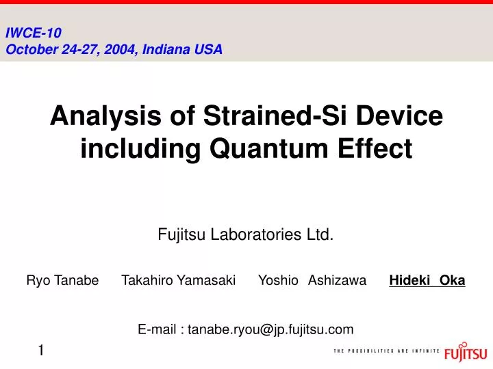
IWCE-10 October 24-27, 2004, Indiana USA. Analysis of Strained-Si Device including Quantum Effect. Fujitsu Laboratories Ltd. Ryo Tanabe Takahiro Yamasaki Yoshio Ashizawa Hideki Oka E-mail : tanabe.ryou@jp.fujitsu.com. Background. z. y. x. tensile strain. tensile strain.

E N D
IWCE-10October 24-27, 2004, Indiana USA Analysis of Strained-Si Device including Quantum Effect Fujitsu Laboratories Ltd. Ryo Tanabe Takahiro Yamasaki YoshioAshizawa HidekiOka E-mail : tanabe.ryou@jp.fujitsu.com
Background z y x tensile strain tensile strain compressive strain Gate Strained Si is studied and used aggressively as one of “Technology Booster” Drain Source Strained Si SiGe buffer layer Si Substrate Is the merit of strain kept with scaling ? ・Quantum Effect・Ballistic Transport The necessity of Strained-Si Monte Carlo simulation including quantum effect.
The Implementation of Strained Band kz ky kx 2.5 ky,kz direction Full band Monte Carlo simulator :FALCON 2 1.5 The first principle band calculation program :PHASE Energy (eV) 1 0.5 kx direction 0 0 0.2 0.4 0.6 0.8 1 k Full band structure of Strained Si Band structure of conduction band near X point with 50% expansion of ky, kz direction. Monte Carlo Analysis We linked the first principle band calculation program to the FUJITSU ensemble full band Monte Carlo simulator FALCON directly
Evaluated Structure ・We calculated below Lg=50nm. ・We used Double Gate structure. Phonon, Impurity and Surface Roughness scattering Lg=40nmTsoi=10nmTox=1nm
Id-Vg@Vd=0.05V ・Vd=0.05V・Drain current is saturated at Ge=20%
Id-Vg@Vd=0.8V ・Vd=0.8V・Drain current is not saturated.
Valley Distribution 2fold 1 Vd=0.05V 0.9 Vd=0.2V 0.8 Vd=0.4V 0.7 Vd=0.6V Vd=0.8V 0.6 Vd=1.0V 0.5 4fold① 0.4 0.3 0.2 0.1 0 2fold 4fold① 4fold② 2fold 4fold① 4fold② 0% 30% 4fold②
The Introduction of Quantum Effect ・We implemented quantum effect by Bohm Potential method Scattering V(r) Eq . (1) V (r) * ・・・(1) Eq . (2) ・・・(2) E(r) V(r):PotentialV*(r):Quantum Corrected PotentialE(r):Electric Field t < t max
L=40nmVg=0.8V, Vd=0V The Comparison with Schrödinger-Poisson Gate Oxide
The Comparison of Scattering Quantum Effect Strain Effect Including quantum effect
Ballistic Rate and Ion Improvement ・Ballistic particles exceed 50% at L=10nm. ・Both ballistic rate and Ion improvement with quantum effect are larger than with classical.
The Comparison of Electron Velocity Source region Vg=Vd=0.8 V 6.0E+07 L=5nm x=0.3 x=0 L=10nm 4.0E+07 L=20nm L=40nm Electron Velocity (cm/sec) 2.0E+07 0.0E+00 -30 -20 -10 0 10 20 30 Position along the channel (nm)
Summary • We linked the first principle band calculation program to full-band MC simulator directly. • We implemented Bohm Potential Quantum correction model and analyzed Strained-Si device including quantum effect. • As gate length is scaled down, Ion improvement by strain effect will decrease, but In the regime that ballistic transport is dominant (about below 10nm), strain effect will increase again due to increasing injection velocity from source region.