Download
1 / 11
110 likes | 277 Views
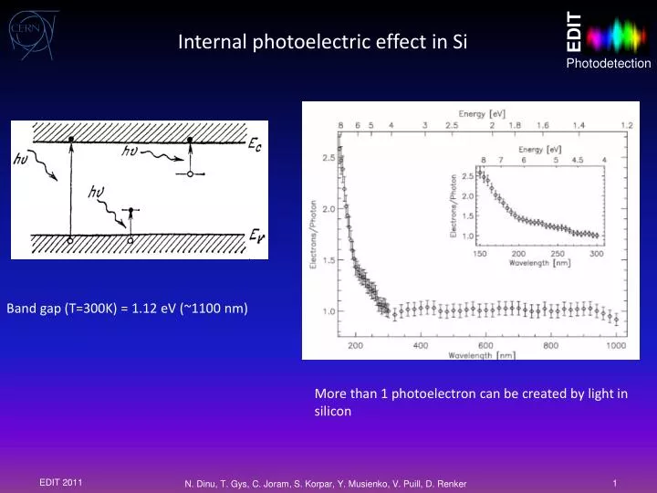
Internal photoelectric effect in Si. Band gap (T=300K) = 1.12 eV (~1100 nm). More than 1 photoelectron can be created by light in silicon. EDIT 2011. 1. N. Dinu, T. Gys, C. Joram, S. Korpar, Y. Musienko, V. Puill, D. Renker. PIN photodiode.

E N D
Internal photoelectric effect in Si Band gap (T=300K) = 1.12 eV (~1100 nm) More than 1 photoelectron can be created by light in silicon EDIT 2011 1 N. Dinu, T. Gys, C. Joram, S. Korpar, Y. Musienko, V. Puill, D. Renker
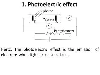
PIN photodiode One of the simplest kind of photodiodes is the p-i-n photodiode in which an intrinsic piece of semiconductor is sandwiched between two heavily (oppositely) doped regions. The two charge sheets (on the n+ and p+) sides produce a field which, even without an external field supplied, will tend to separate charges produced in the depleted region. The separated charges will be swept to either terminal and can be detected as a current provided that they did not recombine. EDIT 2011 2 N. Dinu, T. Gys, C. Joram, S. Korpar, Y. Musienko, V. Puill, D. Renker
Semiconductor devices: PIN photodiodes The PIN diode is a very successful device. It is used in many big calorimeters in high energy physics (Cleo, L3, Crystal Barrel, Barbar, Belle ....) The PIN diode is the simplest, most reliable and cheapest photo sensor. It has high quantum efficiency (80%), very small volume and is insensitive to magnetic fields EDIT 2011 3 N. Dinu, T. Gys, C. Joram, S. Korpar, Y. Musienko, V. Puill, D. Renker
PIN photodiodes – nuclear counter effect rear leakage Geant simulation: each dot stands for an energy deposition of more than 10 keV A MIP in a PIN diode creates ~30,000 e-h pairs (the diode thickness of 300 x 100 pairs/). A photon with an energy of 7 GeV produces in PbWO4 + PIN diode the same number of e-h pairs. 80 GeV e- beam in a 18 cm long PbWO4 crystal N. Dinu, T. Gys, C. Joram, S. Korpar, Y. Musienko, V. Puill, D. Renker EDIT 2011 4
Basic APD Structure (CMS version) Photons create electron-hole pairs in the thin p-layer on top of the device and the electrons induce avalanche amplification in the high field at the p-n junction. Holes created behind the junction contribute little because of their much smaller ionization coefficient. Electrons produced by ionizing particles traversing the bulk are not amplified. The effective thickness for the collection and amplification of electrons which have been created by a MIP is therefore about 6 m ~(5 x 50 + 45 x 1)/50. The NCE is 50 times smaller than in a PIN diode. 50 m Ionization coefficients for electrons and for holes EDIT 2011 5 N. Dinu, T. Gys, C. Joram, S. Korpar, Y. Musienko, V. Puill, D. Renker
APDs in the CMS ECAL 36 supermodules with 1700 crystals each PbWO4 crystal 2 APD’s/crystal 122.400 APD’s
APD Impact on Energy Resolution ECAL energy resolution: CMS design goal :a ~3%, b~0.5%, c~200 MeV APD contributions to: a: photo statistics (area, QE) and avalanche fluctuations (excess noisefactor) b: stability (gain sensitivity to voltage and temperature variation, aging and radiation damage) c: noise (capacitance, serial resistance and dark current)
Gain and Dark Current dM/dV*1/M = const * M M 1/(Vbreakdown - V) Near the breakdown voltage, where we get noticeable amplification, the gain is a steep function of the bias voltage. Consequently we need a voltage supply with a stability of few tens of mV. EDIT 2011 8 N. Dinu, T. Gys, C. Joram, S. Korpar, Y. Musienko, V. Puill, D. Renker
The gain of an APD is limited The breakdown voltage depends on the temperature due to energy loss of the electrons in interactions with phonons.Consequently the gain depends on the temperature and the dependence increases with the gain. At gain 50 the temperature coefficient is - 2.3% per degree C. Good energy resolution can only be achieved when the temperature is kept stable (in CMS the temperature is regulated with a 0.1 degree C precision). At high gain the fluctuations of the gain become large and the excess noise factor ENF increases: ENF = keff • M + (2-1/M) • (1-keff) for M > 10: ENF = 2 + keff • M keff k = / and are the ionization coefficients for electrons and holes ( >> ) N. Dinu, T. Gys, C. Joram, S. Korpar, Y. Musienko, V. Puill, D. Renker EDIT 2011 9
Quantum efficiency (QE) In the APDs selected for CMS (Hamamatsu S8148) the p-n junction is at a depth of about 5 micron. Behind the junction is a 45 micron thick layer of n-doped silicon. Blue light is absorbed close to the surface. The electrons from the generated e-h pairs drift to the high field of the junction and are amplified Light with long wavelength penetrates deep into the region behind the p-n junction. Only the generated holes will drift to the junction. They will be much less amplified due to the smaller ionization coefficient. EDIT 2011 10 N. Dinu, T. Gys, C. Joram, S. Korpar, Y. Musienko, V. Puill, D. Renker
Radiation hardness Two APD’s have been irradiated at PSI in a 70 MeV proton beam for 105 minutes 9x10¹² protons/cm2 corresponds to 2x10¹³ neutrons/cm2 with an energy of 1MeV (10 years fluence expected in CMS barrel) • Neutrons: Displacement of Si atoms => defects in the bulk which generate currents. Slow and never complete recovery at room temperature. • Ionizing radiation (): breakup of the SiO2 molecules and very little effect in the bulk (10-4) => the surface currents increase. Fast and almost complete recovery for good APD‘s. There can be a strong reduction of the breakdown voltage if there is a weakness on the surface due to an imperfection in the production process (dust particles, mask misalignment ...). The mean bulk current after 2x10¹³ neutrons/cm2 is Id280nA (non-amplified value). This corresponds to 14A at gain50 and ~ 80MeV noise contribution (no recovery considered). EDIT 2011 11 N. Dinu, T. Gys, C. Joram, S. Korpar, Y. Musienko, V. Puill, D. Renker