Download
1 / 45
530 likes | 926 Views
Chapter 6 – MSP430 Micro-Architecture. Levels of Transformation. Problems. Algorithms. Language (Program). Programmable. Computer Specific. Machine (ISA) Architecture. Microarchitecture. Manufacturer Specific. Circuits. Devices. Topics to Cover…. MSP430 Micro-Architecture

E N D
Levels of Transformation Problems Algorithms Language (Program) Programmable Computer Specific Machine (ISA) Architecture Microarchitecture Manufacturer Specific Circuits Devices Chapter 6 - MSP430 Micro-Architecture
Topics to Cover… • MSP430 Micro-Architecture • Instruction Cycle Review • Fetch Cycle • Source Addressing Modes • Evaluate Source Operand • Destination Addressing Modes • Evaluate Destination Operand • Execute Cycle • Store Cycle • Instruction Clock Cycles • Digital I/O Chapter 6 - MSP430 Micro-Architecture
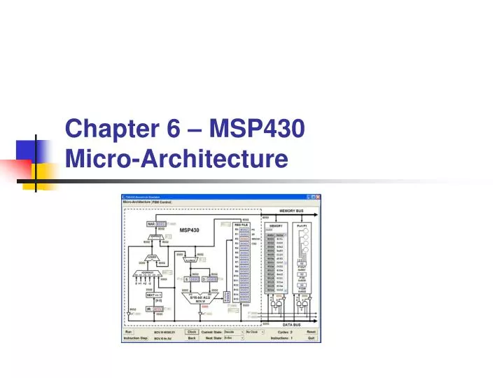
MSP430 Micro-Architecture MSP430 Modular Architecture Chapter 6 - MSP430 Micro-Architecture
MSP430 Micro-Architecture Micro-Architecture Simulator Address Bus Program Counter Memory Address Register Source Operand Instruction Register Destination Operand Port 1 Output Memory Arithmetic Logic Unit Condition Codes Chapter 6 - MSP430 Micro-Architecture Data Bus
Instruction Cycle The Instruction Cycle • INSTRUCTION FETCH • Obtain the next instruction from memory • DECODE • Examine the instruction, and determine how to execute it • SOURCE OPERAND FETCH • Load source operand • DESTINATION OPERAND FETCH • Load destination operand • EXECUTE • Carry out the execution of the instruction • STORE RESULT • Store the result in the designated destination Not all instructions require all six phases Chapter 6 - MSP430 Micro-Architecture
PC Fetch Cycle Fetching an Instruction PC can be incremented anytime during the Fetch phase Chapter 6 - MSP430 Micro-Architecture
Source Addressing Modes Source Addressing Modes • The MSP430 has four basic modes for the source address: • Rs - Register • x(Rs) - Indexed Register • @Rs - Register Indirect • @Rs+ - Indirect Auto-increment • In combination with registers R0-R3, three additional source addressing modes are available: • label - PC Relative, x(PC) • &label – Absolute, x(SR) • #n – Immediate, @PC+ Chapter 6 - MSP430 Micro-Architecture
Evaluate Source Operand Register Addressing Mode Chapter 6 - MSP430 Micro-Architecture
Rs Evaluate Source Operand Source: Register Mode – Rs Select the generic source register Chapter 6 - MSP430 Micro-Architecture
Evaluate Source Operand Register-Indexed Addressing Mode Chapter 6 - MSP430 Micro-Architecture
Rs PC PC Evaluate Source Operand Source: Indexed Mode – x(Rs) PC incremented at end of phase Use PC to obtain index, use Rs for base register Chapter 6 - MSP430 Micro-Architecture
Evaluate Source Operand Symbolic Addressing Mode Chapter 6 - MSP430 Micro-Architecture
PC PC PC Evaluate Source Operand Source: Symbolic Mode – Address PC incremented at end of phase Use PC to obtain relative index and for base register Chapter 6 - MSP430 Micro-Architecture
Evaluate Source Operand Absolute Addressing Mode Chapter 6 - MSP430 Micro-Architecture
Source: Absolute Mode – &Address #0 PC Evaluate Source Operand PC can be incremented anytime during the phase Use PC to obtain absolute address, use #0 for base register BYU CS/ECEn 124 Chapter 6 - MSP430 Micro-Architecture 16
Evaluate Source Operand Register Indirect Addressing Mode Chapter 6 - MSP430 Micro-Architecture
Rs Evaluate Source Operand Source: Indirect Mode – @Rs Chapter 6 - MSP430 Micro-Architecture
Evaluate Source Operand Register Indirect Auto-increment Chapter 6 - MSP430 Micro-Architecture
Source: Indirect Auto Mode – @Rs+ Rs Evaluate Source Operand Increment by 1 (.b) or 2 (.w) BYU CS/ECEn 124 Chapter 6 - MSP430 Micro-Architecture 20
Evaluate Source Operand Immediate Addressing Mode Chapter 6 - MSP430 Micro-Architecture
PC Evaluate Source Operand Source: Immediate Mode – #n PC can be incremented anytime during the phase Chapter 6 - MSP430 Micro-Architecture
MSP430 Source Constants To improve code efficiency, the MSP430 "hardwires" six register/addressing mode combinations to commonly used source values: #0 - R3 in register mode #1 - R3 in indexed mode #4 - R2 in indirect mode #2 - R3 in indirect mode #8 - R2 in indirect auto-increment mode #-1 - R3 in indirect auto-increment mode Eliminates the need to use a memory location for the immediate value - commonly reduces code size by 30%. Evaluate Source Operand BYU CS/ECEn 124 Chapter 6 - MSP430 Micro-Architecture 23
Source: Constant Mode – #1 (-1,0,1,2,4,8) R3 Evaluate Source Operand BYU CS/ECEn 124 Chapter 6 - MSP430 Micro-Architecture 24
Destination Addressing Modes There are two basic modes for the destination address: Rd - Register x(Rd) - Indexed Register In combination with registers R0/R2, two additional destination addressing modes are available: label - PC Relative, x(PC) &label – Absolute, x(SR) Destination Addressing Modes BYU CS/ECEn 124 Chapter 6 - MSP430 Micro-Architecture 25
Destination: Register Mode – Rd Rd Evaluate Destination Operand BYU CS/ECEn 124 Chapter 6 - MSP430 Micro-Architecture 26
Destination: Indexed Mode – x(Rd) Rs PC PC Evaluate Destination Operand PC incremented at end of phase Use PC to obtain index, use Rs for base register BYU CS/ECEn 124 Chapter 6 - MSP430 Micro-Architecture 27
Destination: Absolute Mode – &Address #0 PC Evaluate Destination Operand PC can be incremented anytime during the phase Use PC to obtain absolute address, use #0 for base register BYU CS/ECEn 124 Chapter 6 - MSP430 Micro-Architecture 28
Destination: Symbolic Mode – Address PC PC PC Evaluate Destination Operand PC incremented at end of phase Use PC to obtain relative index and for base register BYU CS/ECEn 124 Chapter 6 - MSP430 Micro-Architecture 29
Final Instruction Phases • Execute • PUSH • Decrement stack pointer (R1) • Ready address for store phase • JUMP • Compute 10-bit, 2’s complement, sign extended • Add to program counter (R0) • Store • Move data from ALU to register, memory, or I/O port BYU CS/ECEn 124 Chapter 6 - MSP430 Micro-Architecture 30
Execute Phase: PUSH.W SP Use Store Phase to push on stack Execute Cycle SP = SP - 2 BYU CS/ECEn 124 Chapter 6 - MSP430 Micro-Architecture 31
PC Execute Cycle Execute Phase: Jump Select “COND” to conditionally change PC 2’s complement, sign-extended Chapter 6 - MSP430 Micro-Architecture
Store Cycle Store Phase: Rd Chapter 6 - MSP430 Micro-Architecture
Store Cycle Store Phase: Other… Chapter 6 - MSP430 Micro-Architecture
Instruction Clock Cycles Instruction Timing • Instruction cycles = Power consumption • Most instruction cycles limited by access to memory (von Neumann bottleneck) • In general • 1 cycle to fetch instruction • +1 cycle for @Rn, @Rn+, or immediate • +2 cycles for indexed, absolute, or symbolic • +1 to write destination back to memory • 2 cycles for any jump • No difference between byte and word Chapter 6 - MSP430 Micro-Architecture
Instruction Clock Cycles Cycles Per Instruction... • Instruction timing: • 1 cycle to fetch instruction word • +1 cycle if source is @Rn, @Rn+, or #Imm • +2 cycles if source uses indexed mode • 1st to fetch base address • 2nd to fetch source • Includes absolute and symbolic modes • +2 cycles if destination uses indexed mode • +1 cycle if writing destination back to memory
Instruction Clock Cycles Cycles Per Instruction... SrcDstCyclesLengthExample Rn Rm 1 1 MOV R5,R8 @Rm 2 1 MOV R5,@R6 x(Rm) 4 2 ADD R5,4(R6) EDE 4 2 XOR R8,EDE &EDE 4 2 MOV R5,&EDE #n x(Rm) 5 3 MOV #100,TAB(R8) &TONI &EDE 6 3 MOV &TONI,&EDE
Quiz Quiz • Given a 1.2 mHz processor, what value for DELAY would result in a 1/2 second delay? DELAY .equ ??? mov.w #DELAY,r12 delay1: dec.w r12 jn delay3 mov.w #1000,r15 delay2: dec.w r15 jne delay2 jmp delay1 delay3:
Digital I/O Digital I/O • Digital I/O grouped in 8 bit memory locations called ports • Each I/O port can be: • programmed independently for each bit • combined for input, output, and interrupt functionality • Edge-selectable input interrupt capability for all 8 bits of ports P1 and P2 • Read/write access using regular MSP430 byte instructions • Individually programmable pull-up/pull-down resistors • The available digital I/O pins for the hardware development tools: • eZ430-F2013: 10 pins - P1 (8 bits) and P2 (2 bits); • eZ430-F2274: 32 pins – P1, P2, P3, and P4 Chapter 6 - MSP430 Micro-Architecture
Digital I/O 8-bit Digital I/O Registers • Direction Register (PxDIR): • Bit = 1: the individual port pin is set as an output • Bit = 0: the individual port pin is set as an input • Input Register (PxIN): • When pins are configured as GPIO, each bit of these read-only registers reflects the input signal at the corresponding I/O pin • Bit = 1: The input is high • Bit = 0: The input is low • Output Register (PxOUT): • Each bit of these registers reflects the value written to the corresponding output pin. • Bit = 1: The output is high; • Bit = 0: The output is low. • Note: the PxOUT is a read-write register which means previously written values can be read, modified, and written back Chapter 6 - MSP430 Micro-Architecture
Digital I/O Select Digital I/O Registers • Function Select Registers: (PxSEL) and (PxSEL2): • Port P2.0 Example: Chapter 6 - MSP430 Micro-Architecture
Digital I/O Interrupt Digital I/O Registers • Interrupt Enable (PxIE): • Read-write register to enable interrupts on individual pins on ports P1/P2 • Bit = 1: The interrupt is enabled • Bit = 0: The interrupt is disabled • Each PxIE bit enables the interrupt request associated with the corresponding PxIFG interrupt flag • Interrupt Edge Select Registers (PxIES): • Selects the transition on which an interrupt occurs • Bit = 1: Interrupt flag is set on a high-to-low transition • Bit = 0: Interrupt flag is set on a low-to-high transition • Interrupt Flag Registers (PxIFG) • Set automatically when the programmed signal transition (edge) occurs • PxIFG flag can be set and must be reset by software • Bit = 0: No interrupt is pending • Bit = 1: An interrupt is pending Chapter 6 - MSP430 Micro-Architecture
+3.3v P2.0 P2.1 P2.2 P2.3 P2.4 Digital I/O Pull-up/down Register • Pull-up/down Resistor Enable Registers (PxREN): • Each bit of this register enables or disables the pull-up/pull-down resistor of the corresponding I/O pin • Bit = 1: Pull-up/pull-down resistor enabled • Bit = 0: Pull-up/pull-down resistor disabled. • When pull-up/pull-down resistor is enabled, Output Register (PxOUT) selects: • Bit = 1: The pin is pulled up • Bit = 0: The pin is pulled down. Chapter 6 - MSP430 Micro-Architecture
Digital I/O Port P1 Registers Chapter 6 - MSP430 Micro-Architecture