Download
1 / 50
500 likes | 629 Views
Photoemission Studies of Interface Effects on Thin Film Properties. Final Examination April 18 th , 2006 Dominic A. Ricci Department of Physics University of Illinois at Urbana-Champaign. Threshold of Technology. 1947. 10 -1 m. 2006. 10 -7 m. 2020. 10 -9 m. Year. Length Scale.

E N D
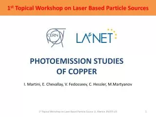
Photoemission Studies of Interface Effects on Thin Film Properties Final Examination April 18th, 2006 Dominic A. Ricci Department of Physics University of Illinois at Urbana-Champaign
Threshold of Technology 1947 10-1 m 2006 10-7 m 2020 10-9 m Year Length Scale 3.5 million transistors Final examination, April 18, 2006
On the Atomic Scale When physical structures < e- coherence length quantum effects manifest 1D e- confinement quantum well states Thin films Pure Science Applied Technology Quantum wells dominate properties of thin films Understand quantum physics of thin films Thin films are building blocks Final examination, April 18, 2006
Film Properties • Schottky barrier height • Rectifying energy barrier at metal-semiconductor junction • Confines electrons in film • Determines transport properties in solid-state devices • Thermal stability temperature • Annealing temperature at which smooth film structure roughens • Relevant to robustness under technological operating conditions Final examination, April 18, 2006
Preview Thin Pb films grown on metal (Au, In, Pb)-terminated Si(111) probed with angle-resolved UV photoemission • Terminating metal serves as interfactant layer between film and substrate • Quantum well states depend on boundary conditions • Same film, same substrate, different interfactant – isolates the interface effect on properties • Schottky barrier and thermal stability measured via quantum well spectroscopy Control electronic and physical film properties with interfacial engineering Final examination, April 18, 2006
Overview • Background • Photoemission • Surfaces reconstructions and films • Quantum well states • Results • Schottky barrier tuning • Thermal stability temperature control Final examination, April 18, 2006
Photoemission Spectroscopy • Probes electronic states in system • Input: High intensity, monochromatic photons (VUV) • Output: e- emitted – energy, momentum recorded • (angle-resolved) e- = photoelectron kinetic energy = electronic state binding energy = work function Final examination, April 18, 2006
Photoemission Spectroscopy • Probes electronic states in system • Input: High intensity, monochromatic photons (VUV) • Output: e- emitted – energy, momentum recorded • (angle-resolved) e- Normal emission hν = 22 eV Photoemission is surface sensitive – ideal for studying thin films Final examination, April 18, 2006
Photoemission Spectrum EF Typical spectrum – energy relative to Fermi level EF Final examination, April 18, 2006
Photoemission Requirements • High intensity monochromatic light • Sample cleanliness • Electron detection Synchrotron Radiation Center (Stoughton, WI) Ultrahigh vacuum chamber (base pressure: 8 x 10-11 torr) Hemispherical electron energy analyzer Final examination, April 18, 2006
Overview • Background • Photoemission • Surfaces reconstructions and films • Quantum well states • Results • Schottky barrier tuning • Thermal stability temperature control Final examination, April 18, 2006
Substrate Semiconductor substrate: n-type Si(111) – 7 x 7 • n-type: e- charge carrier • (111): surface plane in Miller indices • 7 x 7 : surface reconstruction periodicity • (n x m): n bulk units by m bulk units relative • to surface 1 x 1 unit cell • Formed by heating in vacuo @ 1250°C for 7-10 s • Si has band gap Eg = 1.15 eV Final examination, April 18, 2006
Deposition Sample • Metal deposited on clean Si(111) surface with molecular beam epitaxy (MBE) • Material evaporated from e-beam-heated crucible • Amount deposited measured in monolayers (ML) • Atomic layer HV Filament Supply Final examination, April 18, 2006
Reconstructions Sub-monolayer amounts of metal are deposited on clean Si(111)-7 x 7 at RT, then annealed, to form reconstructions Used to modify film-substrate boundary Final examination, April 18, 2006
Pb Film Growth Pb Si Metal-reconstructed Si(111) substrates cooled to 60-100 K prior to Pb deposition, then film annealed to 100 K Interfactant • Pb is a free-electron-like metal • Pb/Si interface abrupt w/o intermixing Final examination, April 18, 2006
Overview • Background • Photoemission • Surfaces reconstructions and films • Quantum well states • Results • Schottky barrier tuning • Thermal stability temperature control Final examination, April 18, 2006
Quantum Well States Pb - - e e Si • Metal e- confined in film between vacuum and semiconductor band gap • “Particle-in-a-box” – discrete energies at integer monolayer film thicknesses • Different film thicknesses N • different energies • Different boundary conditions • different energies hv Vacuum Band Gap Final examination, April 18, 2006
Quantum Well States Pb Fermi Level Energy (eV) Si VBM Si L Γ L k(E) Well depth = confinement range E0 between Pb EF and Si valence band maximum CBM EF Eg E0 VBM n-type Semiconductor Metal Final examination, April 18, 2006
Quantum Well States Confined electrons sharp, intense peaks in spectra Energy (eV) E0 E EF Partially confined electrons E < E0 Quantum well resonances broad, less intense peaks Final examination, April 18, 2006
Atomic Layer Resolution • Quantum well peak reaches max intensity at integer monolayer film thickness • Absolute film thickness determination Final examination, April 18, 2006
Bohr-Sommerfeld Phase Model = number ML = ML thickness (Å) = quantum number = e- momentum = surface phase shift = interface phase shift boundary dependence Total electronic phase quantized in 2π Quantum well state energy levels for (N, n) Final examination, April 18, 2006
Overview • Background • Photoemission • Surfaces reconstructions and films • Quantum well states • Results • Schottky barrier tuning • Thermal stability temperature control Final examination, April 18, 2006
Schottky Barrier Schottky Barrier • Rectifying energy barrier at metal-semiconductor junction • Barrier height S = Eg – E0 for n-type substrate CBM EF E0 Eg VBM Examine Schottky barrier height by varying film-substrate boundary condition n-type Semiconductor Metal Final examination, April 18, 2006
Measuring the Barrier Height Measure E0 Measure S • Two methods using quantum well spectroscopy: • Energy level analysis • Interface phase shift depends on E0 • Fit energy levels to obtain barrier height • Peak width analysis • E0 < E < EF: small width; E < E0: larger width • Identify threshold to obtain barrier height Final examination, April 18, 2006
Energy Level Analysis Normal emission spectra Pb/Au-6x6/Si(111) @ 100 K • Energy levels differ by ~1 eV among systems • known from first-principles calculations • (singularity at VBM) • Simultaneous fit E(N,n) • obtain E0 for all systems Final examination, April 18, 2006
Peak Width Analysis Peak Width (eV) Energy (eV) • Widths increase rapidly below E0 threshold • provides measurement of Schottky barrier • Weighted avg. with heights from energy level measurements Differences observed among systems due to interface effect Final examination, April 18, 2006
Interface Dipole Model - + Pb Pb Pb Pb Pb Pb Au Au Pb Au Au Au Si Si Si Si Si Si Si Si Si Si Si Si - + Interface species concentration and electronegativity determine charge transfer around metal-semiconductor dipoles Final examination, April 18, 2006
Interface Dipole Model - + Pb Pb Pb Pb Pb Pb Au Au Pb Au Au Au Si Si Si Si Si Si Si Si Si Si Si Si - + Interface species concentration and electronegativity determine charge transfer around metal-semiconductor dipoles • = avg. charge state of interfacial Si • = electronegativity • = interfactant concentration Final examination, April 18, 2006
Interface Dipole Model - + Pb Pb Pb Pb Pb Pb Au Au Pb Au Au Au Si Si Si Si Si Si Si Si Si Si Si Si - + Interface species concentration and electronegativity determine charge transfer around metal-semiconductor dipoles • = avg. charge state of interfacial Si • = electronegativity • = interfactant concentration • = Schottky barrier height from model Final examination, April 18, 2006
Schottky Barrier Results Comparison of Sexp (circles) to Scalc (line) yields agreement Interface dipole model reproduces measurements with only chemical parameters (concentration, electronegativity) Schottky barrier tuning via proper interfactant selection Final examination, April 18, 2006
Overview • Background • Photoemission • Surfaces reconstructions and films • Quantum well states • Results • Schottky barrier tuning • Thermal stability temperature control Final examination, April 18, 2006
Thermal Stability Temperature Annealing temperature at which smooth film structure roughens Thermal energy allows atomic rearrangement T > Tstability T < Tstability Compare Pb films w/ 3 interfactants: Final examination, April 18, 2006
Electronic Stability Quantized electronic structure Total film electronic energy Thermal stability • Quantum well energy levels change with N • Layer-to-layer variation in total electronic energy • Thickness-dependent thermal stability Final examination, April 18, 2006
Thickness Oscillations in Pb Films • e- fill quantum wells w/ increasing N • “Shell effect” – periodic oscillation in total energy and film properties • ΔN = 2.2 ML @ integer sampling • Beating pattern • Characteristic oscillation in work function, charge density distribution, interlayer lattice spacing, TC Final examination, April 18, 2006
Quantum Well Spectroscopy Redux Interface phase shift In Au Pb A = -1.70 0.29 2.21 • In and Pb diff. by ~π • ΔN = 1 equivalent to phase change of π Final examination, April 18, 2006
Measuring Thermal Stability • Quantum well peak intensity monitored as function of T as film annealed • Sudden drop off at Tstability as film rearranges to more stable thicknesses Final examination, April 18, 2006
Thermal Stability Analysis • Oscillation phase reversal in Pb/In/Si(111) system • odd N more stable • Oscillation amplitude larger in Pb/Au/Si(111) system • stable above RT Final examination, April 18, 2006
Thermal Stability Analysis In Au Pb Φ = -1.354 0.942 1.529 • In and Pb diff. by ~π Friedel-like functional form: Φ = phase shift (interfactant dependent) Thermal stability control via interfacial engineering Final examination, April 18, 2006
Recapitulation Thin Pb films grown on metal (Au, In, Pb)-terminated Si(111) probed with angle-resolved UV photoemission • Used interfactant layers to alter film-substrate boundary condition and change film quantum electronic structure • Schottky barrier tuning • Thermal stability temperature manipulation Control electronic and physical film properties with interfacial engineering Final examination, April 18, 2006
Title Final examination, April 18, 2006
Future Directions • Pure science • Use quantum well spectroscopy to probe other film properties to identify non-classical behavior • Applications to technology • Control film properties, e.g. superconducting TC Final examination, April 18, 2006
Synchrotron Radiation • High intensity monochromatic light Synchrotron Radiation Center (Stoughton, WI) • Magnet-confined e- ring • Monochrometers at beamlines Final examination, April 18, 2006
Ultrahigh Vacuum • Sample cleanliness Ultrahigh vacuum chamber (base pressure: 8 x 10-11 torr) • UHV < 10-9 torr • Stainless steel chamber • Series of pumps Final examination, April 18, 2006
Energy Analyzer e- Focusing Lenses R0 • Electron detection Sample Hemispherical electron energy analyzer Slits R1 R2 Detector/ CCD Camera Final examination, April 18, 2006
Deposition Sample XTM Current Monitor Crucible HV Filament Feedback Control Filament Supply Metal deposited on clean Si(111) surface with molecular beam epitaxy • Amount deposited measured in • monolayers (ML) • For reconstruction, defined in substrate units: • 1 ML = 7.83 x 10¹⁴ atoms/cm2 for Si(111) surface • For film, defined by bulk: • 1 ML = 9.43 x 10¹⁴ atoms/cm2 for • Pb(111) films Final examination, April 18, 2006
RHEED Sample on Rotatable Manipulator 10 keV electron gun RHEED Pattern on Phosphor Screen Surface quality monitored with Reflection High Energy Electron Diffraction (RHEED) Final examination, April 18, 2006
Phase Comparison lags by ~π/2 Direct relationship Thermal stability control via interfacial engineering Final examination, April 18, 2006
Thermal Stability Analysis Friedel-like functional form: α = 1.77 from free electron model Φ = phase shift (interfactant dependent) In Au Pb Φ = -1.354 0.942 1.529 • In and Pb diff. by ~π Final examination, April 18, 2006
Phase Comparison Direct relationship Φ can be determined from quantum well energy levels Thermal stability control via interfacial engineering Final examination, April 18, 2006