Download

1 / 95
1.09k likes | 1.45k Views
Bipolar Junction Transistors (BJTs). 1. Electronics Concept. THE PAST. 1904 Flemming invented a value-Diode Cathode & Anode Positive voltages at Anode; current flows Negative voltages at Anode; No current flows Acted as Detector 1906 De Forset

E N D
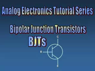
Bipolar Junction Transistors (BJTs) 1
THE PAST • 1904 Flemming • invented a value-Diode • Cathode & Anode • Positive voltages at Anode; current flows • Negative voltages at Anode; No current flows • Acted as Detector • 1906 De Forset • Put a third electrode in between and small change in voltage on the grid resulted in a large plate voltage change. • Acted as an amplifier • Vacuum Tubes not reliable
Solid State Components • December 1947 • Closely space two gold-wires probes were pressed into the surface of a germanium crystal and amplification of input voltages experienced. • Low gain, low bandwidth and Noisy • 1947 - 1950 • Junction Transistor invented where the operation depended upon diffusion instead of conduction current. • Had charged carrier of both polarities -- Electron and Holes • 1951 • Solid state transistors were produced commercially. • Transistor characteristics vary greatly with changes in temperature. Germanium had excessive variations above 750 C, thus Silicon transistor were invented as Silicon Transistors could be used up to 2000 C
The Integrated Circuit • 1958 • Kilby conceived the monolithic idea – Building entire circuit out of Germanium or Silicon • Phase-Shift Oscillator, Multivibrator were build from Germanium with thermally bonded gold connecting wires. • Noyce manufactured multiple devices on a single piece of Silicon and was able to reduced the size, weight and cost per active element.
Technological Advances • 1960 - Small Scale Integration (SSI) • less than100 components per chip • 1966 - Medium Scale Integration (MSI) • More than 100 less than 1000 components per chip • 1969 - Large Scale Integration (LSI) • More than 1000 less than 10,000 components per chip • 1975 - Very Large Scale Integration (VLSI) • More than 10,000 components per chip
INTRODUCTION - BJT • Three terminal device • Basic Principle • Voltage between two terminals controls current flowing in the third terminal. • Device is used in discrete and integrated circuits and can act as : • Amplifier • Logic Gates • Memory Circuits • Switches • Invented in 1948 at Bell Telephone Industries
INTRODUCTION • MOSFET has taken over BJT since 1970’s for designing of integrated circuits but still BJT performance under sever environment is much better than MOSFET e.g. Automotive Electronics • BJT is used in • Very high frequency applications (Wireless Comm) • Very high speed digital logics circuit (Emitter Coupled Logic) • Innovative circuit combine MOSFET being high-input resistance and low power operating devices with BJT merits of being high current handling capacity and very high frequency operation – known as BiMOS or BiCMOS
INTRODUCTION • Study would include • Physical operation of BJT • Terminal Characteristics • Circuit Models • Analysis and design of transistor circuits
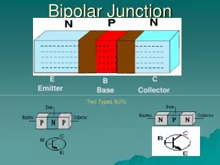
Device Structure & Physical Operation • npn & pnp Transistor • Three terminal ---- Emitter, Base, Collector • Consists of two pn junctions • np-pn -------- npn • pn-np -------- pnp • Modes • Cutoff, Active, Saturation, Reverse Active • Junctions • Emitter Base Junction (EBJ) • Collector-Base Junction (CBJ)
Current flow in an npn transistor biased to operate in the active mode.
npn Transistor • Current in Forward biased junction in active mode: • Emitter Current (IE) flows out of the emitter • Base Current (IB) flows into the Base • Collector Current (IC) flows into the Collector • Majority carriers are electrons as emitter junction is heavily doped and is wider than the base junction, and base junction being lightly doped and has smaller area.
Current Flow • EBJ – Forward Biased, CBJ – Reversed Biased • Only diffusion current is considered as drift current due to thermally generated minority carriers is very small. • Current components across the EBJ are due to: • Electrons injected from the emitter into the base • This current component is at higher level due to heavily doped emitter • High density of electrons in emitter • Holes injected from the base into the emitter • This current component is small due to lightly doped base • Low density of holes in base
Profiles of minority-carrier concentrations in the base and in the emitter of an npn transistor operating in the active mode: vBE > 0 and vCB³ 0.
npn Transistor : Collector Current IC is independent of VCE, as long as the CBJ is reversed biased – collector is positive w.r.t base • IS(Saturation Current) is • Inversely proportional to the base width • Directly proportional to the area of the EBJ • Typical range 10 -12 ---- 10 -18 A • Varies with changes in temperature (Doubles @ every 50 C rise in temperature)
npn Transistor : Base Current iB=iC/β • β (Beta) Common emitter current gain • Ranges from 50 –200 • Constant for a particular transistor • Influenced by : • Width of the base junction(W) • Relative doping of base region w.r.t. emitter region
npn Transistor : Emitter Current • α(Common – Base Current Gain) is • constant for a particular transistor • Less or close to unity • Small change in α corresponds to a very large change in β
Large-signal equivalent-circuit models of the npn BJT operating in the forward active mode.
Model for the npn transistor when operated in the reverse active mode (i.e., with the CBJ forward biased and the EBJ reverse biased).
Equivalent Circuit model • vBE – forward biased EBJ causing an exponentially related current iC to flow • iCis independent of value of the collector voltageas long as CBJ is reversed biased. vCB ≥ 0 V • Collector terminal behaves as an ideal constant current source and its value is determined by vBE iC = αiE
The iC –vCB characteristic of an npn transistor fed with a constant emitter current IE. The transistor enters the saturation mode of operation for vCB< –0.4 V, and the collector current diminishes.
Current flow in a pnp transistor biased to operate in the active mode.
Large-signal model for the pnp transistor operating in the active mode.
Current flow in a pnp & npn transistor biased to operate in the active mode.
Large-signal model for the pnp & npn transistor operating in the active mode.
Figure 5.16 The iC –vBE characteristic for an npn transistor.
Figure 5.17 Effect of temperature on the iC–vBE characteristic. At a constant emitter current (broken line), vBE changes by –2 mV/°C.
Common Base Characteristics • iC – vCB for various iE • Base at constant voltage – grounded thus acts a common terminal potential • Curve is not horizontal straight line but has a small positive slop. iC depends slightly on vCB • At relatively large vCB, iC shows rapid increases – Breakdown phenomena curve
Common Base Characteristics • Intersects the vertical axis at a current equal to • Small signal or incremental can be determined by due to at constant
The Early Effect • In real world • (a) Collector current does show some dependence on collector voltage • (b) Characteristics are not perfectly horizontal line iC - vCE
Figure 5.19 (a) Conceptual circuit for measuring the iC –vCE characteristics of the BJT. (b) The iC –vCE characteristics of a practical BJT.
Emitter serves as a common terminal between input and output terminal Common Emitter Characteristics (ic-vCE) can be obtained at different value of vBE and varying vCE (dc), Collector current can be measured Common Emitter Configuration
The Early Effect • vCE < - 0.4 V CBJ become forward biased & BJT leaves active mode & enters saturation mode • Characteristics is still a straight line but with a finite slope • when extra-polated, the characteristics lines meet at a point on the negative vCE axis @ vCE = -VA • Typical value of VA ranges 50-100v & called early voltage, after the name of english scientist JM Early
The Early Effect • At given vBE , increasing vCE increases reverse biased voltage on CBJ & thus depletion region increases, Resulting in a decrease in the effective base width W • Is is inversely proportional to the base width • Is increases , and Ic also increases proportionally • called Early Effect