Download

1 / 71
720 likes | 885 Views
Chapter 6. Bipolar Junction Transistors (BJTs). Bipolar Junction Transistor. Three terminal device Voltage between two terminals to control current flow in third terminal Invented in 1948 at Bell Telephone Laboratories Dominant until late 1980’s Reliable under harsh operating conditions

E N D
Bipolar Junction Transistor • Three terminal device • Voltage between two terminals to control current flow in third terminal • Invented in 1948 at Bell Telephone Laboratories • Dominant until late 1980’s • Reliable under harsh operating conditions • High frequency applications • High speed designs • High power applications
npn transistor • n-type emitter (E) region, p-type base (B) region, n-type collector (C) region • Two pn junctions (naming basis for bipolar junction transistor) • Modes • Active: used for amplifier design • Cutoff • Saturation: used for logic design • Reverse active: limited operation
Practical Implementation E and C are not symmetrical. pnp transistors works dual to npn transistors much in the same way PMOSFET works dual to NMOSFET. (In this class, we will concentrate on npn transistors.)
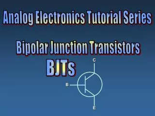
Circuit Symbols for npn Transistors Biasing in active mode Directions of current flow
iC – vBECharacteristics Temperature Dependence
Common Base Characteristics In active region, vCB ≥ - 0.4 V Base voltage is fixed at zero.
Quiescent point must be selected to give a symmetric output swing.
Input part 10 V RB1 RBB RB1 + VBB + + 10 V RB2 _ _ VBB VBB _ RB2
Biasing BJT • Determining a quiescent point for linearization • Active mode operation • Considerations • Stable with respect to manufacturing parameters (e.g., ro, β) • Desired gains • Acceptable output swing
Biasing with Single Power Supply • Fix VBE or IB. • Output directly depends on β • Unstable with respect to temperature variation
Small Signal Analysis • A quiescent point has been determined by biasing. • Active mode operation • Forward biasing for base-emitter junction by VBE • Reverse biasing for collector-base junction by RC and VCC
The transistor performs as a voltage controlled current source with gain gm when input varies by 10 mV or less.
Hybrid π Model • Short circuit voltage sources • Open circuit current sources • Short circuit capacitors