Download
1 / 33
340 likes | 467 Views
Rethinking DRAM Design and Organization for Energy-Constrained Multi-Cores. Aniruddha N. Udipi, Naveen Muralimanohar*, Niladrish Chatterjee, Rajeev Balasubramonian, Al Davis, Norm Jouppi * University of Utah and *HP Labs. Why a complete DRAM redesign?. JEDEC SDRAM Standard.

E N D
Rethinking DRAM Design and Organization for Energy-Constrained Multi-Cores Aniruddha N. Udipi, Naveen Muralimanohar*, Niladrish Chatterjee, Rajeev Balasubramonian, Al Davis, Norm Jouppi* University of Utah and *HP Labs
Why a complete DRAM redesign? JEDEC SDRAM Standard High Density June 1994 Cost-per-bit over time Low Cost-per-bit Energy efficient Time for DRAM’s own “right-hand turn” Rethink design for modern constraints Courtesy: http://www.iiasa.ac.at
Memory Trends Energy Large scale systems attribute 25-40% of total power to the memory subsystem Capital acquisition costs = operating costs over 3 years Energy is a first-order design constraint Access patterns Increasing socket, core, and thread counts Final memory request stream extremely random Cannot design for locality
Memory Trends Energy Large scale systems attribute 25-40% of total power to the memory subsystem Capital acquisition costs = operating costs over 3 years Energy is a first-order design constraint Access patterns Increasing socket, core, and thread counts Final memory request stream extremely random Cannot design for locality What is exact overfetch degree? DRAM Reliability Critical apps require chipkill-level reliability Building fault-tolerance out of unreliable components is expensive Schroeder et al., SIGMETRICS 2009
Related Work • Overfetch • Ahn et al. (SC ’09), Ware et al. (ICCD ’06), Sudan et al. (ASPLOS ’10) • DRAM Low-power modes • Hur et al. (HPCA ’08), Fan et al. (ISLPED ’01), Pandey et al. (HPCA ’06) • DRAM Redesign • Loh (ISCA ’08), Beamer et al. (ISCA ’10) • Chipkill mechanisms • Yoon and Erez (ASPLOS ’10)
Executive Summary • Rethink DRAM design for modern constraints • Low-locality, reduced energy consumption, optimize TCO • Selective Bitline Activation (SBA) • Minimal design changes • Considerable dynamic energy reductions for small latency and area penalties • Single Subarray Access (SSA) • Significant changes to memory interface • Large dynamic and static energy savings • Chipkill-level reliability • Reduced energy and storage overheads for reliability
Outline • DRAM systems overview • Selective Bitline Activation (SBA) • Single Subarray Access (SSA) • Chipkill-level reliability • Conclusion
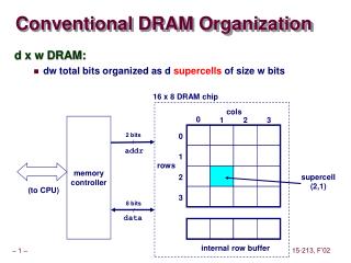
Basic Organization … Array 1/8th of the row buffer One word of data output DRAM chip or device DIMM Rank Bank Memory bus or channel On-chip Memory Controller
Basic DRAM Operation DRAM Chip DRAM Chip DRAM Chip DRAM Chip RAS CAS Cache Line Row Buffer One bank shown in each chip
Outline • DRAM systems overview • Selective Bitline Activation (SBA) • Single Subarray Access (SSA) • Chipkill-level reliability • Conclusion
Selective Bitline Activation • Activate only those bitlines corresponding to the requested cache line – reduce dynamic energy • Some area overhead depending on access granularity • we pick 16 cache lines for 12.5% area overhead • Requires no changes to the interface and minimal control changes
Outline • DRAM systems overview • Selective Bitline Activation (SBA) • Single Subarray Access (SSA) • Chipkill-level reliability • Conclusion
Key Idea Energy-efficient light bulb Higher purchase cost Much lower operating cost Value-addition $0.30 60W $3.00 13W • Incandescent light bulb • Low purchase cost • High operating cost • Commodity It’s worth a small increase in capital costs to gain large reductions in operating costs And not 10X, just 15-20%!
Wishlist of features • Eliminate overfetch • Disregard locality • Increase opportunities for power-down • Increase parallelism • Enable efficient reliability mechanisms
SSA Architecture ONE DRAM CHIP ADDR/CMD BUS DIMM 64 Bytes Subarray Bitlines Bank Row buffer 8 8 8 8 8 8 8 8 8 DATA BUS MEMORY CONTROLLER Global Interconnect to I/O
SSA Basics • Entire DRAM chip divided into small subarrays • Width of each subarray is exactly one cache line • Fetchentirecache line from a single subarray in a single DRAM chip – SSA • Groups of subarrays combined into “banks” to keep peripheral circuit overheads low • Close page policy and “posted-RAS” similar to SBA • Data bus to processor essentially split into 8 narrow buses
SSA Operation DRAM Chip DRAM Chip DRAM Chip DRAM Chip Subarray Subarray Subarray Subarray Subarray Subarray Subarray Subarray Address Subarray Subarray Subarray Subarray Subarray Subarray Subarray Subarray Sleep Mode (or other parallel accesses) Cache Line
SSA Impact • Energy reduction • Dynamic – fewer bitlines activated • Static – smaller activation footprint – more and longer spells of inactivity – better power down • Latency impact • Limited pins per cache line – serialization latency • Higher bank-level parallelism – shorter queuing delays • Area increase • More peripheral circuitry and I/O at finer granularities – area overhead (< 5%)
Methodology • Simics based simulator • ‘ooo-micro-arch’ and ‘trans-staller’ • FCFS/FR-FCFS scheduling policies • Address mapping and DRAM models from DRAMSim • DRAM data from Micron datasheets • Area/Energy numbers from heavily modified CACTI 6.5 • PARSEC/NAS/STREAM benchmarks • 8 single-threaded OOO cores, 32 KB L1, 2 MB L2 • 2GHz processor, 400MHz DRAM
Dynamic Energy Reduction Moving to close page policy – 73% energy increase on average Compared to open page, 3X reduction with SBA, 6.4X with SSA
Contributors to energy consumption 64 cache lines in baseline 16 cache lines in SBA 1 cache line in SSA
Static Energy – Power down modes • Current DRAM chips already support several low-power modes • Consider the low-overhead power down mode: 5.5X lower energy, 3 cycle wakeup time • For a constant 5% latency increase • 17% low-power operation in the baseline • 80% low-power operation in SSA
Latency Characteristics • Impact of Open/Close page policy – 17% decrease (10/12) or 28% increase (2/12) • Posted-RAS adds about 10% • Serialization/Queuing delay balance in SSA - 30% decrease (6/12) or 40% increase (6/12)
Outline • DRAM systems overview • Selective Bitline Activation (SBA) • Single Subarray Access (SSA) • Chipkill-level reliability • Conclusion
DRAM Reliability • Many server applications require chipkill-level reliability – failure of an entire DRAM chip • One example of existing systems • 64-bit word requires 8-bit ECC • Each of these 72 bits must be read out of a different chip, else a chip failure will lead to a multi-bit error in the 72-bit field – unrecoverable! • Reading 72 chips - significant overfetch! • Chipkill even more of a concern for SSA since entire cache line comes from a single chip
Proposed Solution DIMM DRAM DEVICE Approach similar to RAID-5 L0 C L1 C L2 C L3 C L4 C L5 C L6 C L7 C P0 C L9 C L10 C L11 C L12 C L13 C L14 C L15 C P1 C L8 C .. .. .. .. .. .. .. .. .. P7 C L56 C L57 C L58 C L59 C L60 C L61 C L62 C L63 C L – Cache Line C – Local Checksum P – Global Parity
Chipkill design • Two-tier error protection • Tier - 1 protection – self-contained error detection • 8-bit checksum/cache line – 1.625% storage overhead • Every cache line read is now slightly longer • Tear -2 protection – global error correction • RAID-like striped parity across 8+1 chips • 12.5% storage overhead • Error-free access (common case) • 1 chip reads • 2 chip writes – leads to some bank contention • 12% IPC degradation • Erroneous access • 9 chip operation
Outline • DRAM systems overview • Selective Bitline Activation (SBA) • Single Subarray Access (SSA) • Chipkill-level reliability • Conclusion
Key Contributions • Redesign of DRAM microarchitecture • Substantial chip access energy savings (up to 6X) • Overall, performance is a wash • Minor area impact (12% with SBA, 4.5% with SSA) • Two-tier chipkill-level reliability with minimal energy and storage overheads
Now is the time for new architectures.. • Take into account modern constraints • Energy far more critical today than before • Cost-per-bit perhaps less important – optimize TCO • Operating costs over 3 years = capital acquisition costs • Memory reliability is important for many server applications. Memory system’s “right-hand-turn” is long overdue