Download
1 / 64
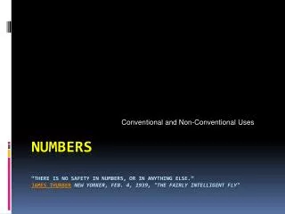
820 likes | 1.29k Views
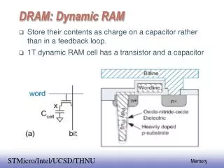
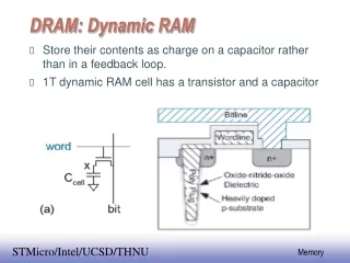
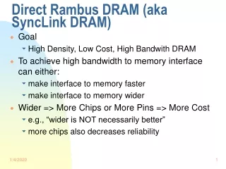
Conventional DRAM Organization. d x w DRAM: dw total bits organized as d supercells of size w bits. 16 x 8 DRAM chip. cols. 0. 1. 2. 3. memory controller. 0. 2 bits /. addr. 1. rows. supercell (2,1). 2. (to CPU). 3. 8 bits /. data. internal row buffer.

E N D
Conventional DRAM Organization d x w DRAM: • dw total bits organized as d supercells of size w bits 16 x 8 DRAM chip cols 0 1 2 3 memory controller 0 2 bits / addr 1 rows supercell (2,1) 2 (to CPU) 3 8 bits / data internal row buffer
Reading DRAM Supercell (2,1) Step 1(a): Row access strobe (RAS) selects row 2. Step 1(b): Row 2 copied from DRAM array to row buffer. 16 x 8 DRAM chip cols 0 memory controller 1 2 3 RAS = 2 2 / 0 addr 1 rows 2 3 8 / data internal row buffer
To CPU supercell (2,1) supercell (2,1) Reading DRAM Supercell (2,1) Step 2(a): Column access strobe (CAS) selects column 1. Step 2(b): Supercell (2,1) copied from buffer to data lines, and eventually back to the CPU. 16 x 8 DRAM chip cols 0 memory controller 1 2 3 CAS = 1 2 / 0 addr 1 rows 2 3 8 / data internal row buffer internal buffer
addr (row = i, col = j) bits 56-63 bits 48-55 bits 40-47 bits 32-39 bits 24-31 bits 16-23 bits 8-15 bits 0-7 63 63 56 56 55 55 48 48 47 47 40 40 39 39 32 32 31 31 24 24 23 23 16 16 15 15 8 8 7 7 0 0 64-bit doubleword at main memory address A 64-bit doubleword at main memory address A 64-bit doubleword Memory Modules : supercell (i,j) DRAM 0 64 MB memory module consisting of eight 8Mx8 DRAMs DRAM 7 Memory controller
Typical Bus Structure Connecting CPU and Memory A bus is a collection of parallel wires that carry address, data, and control signals. Buses are typically shared by multiple devices. CPU chip register file ALU system bus memory bus main memory bus interface I/O bridge
Memory Read Transaction (1) CPU places address A on the memory bus. register file Load operation:movl A, %eax ALU %eax main memory 0 I/O bridge A bus interface A x
Memory Read Transaction (2) Main memory reads A from the memory bus, retreives word x, and places it on the bus. register file Load operation:movl A, %eax ALU %eax main memory 0 I/O bridge x bus interface A x
Memory Read Transaction (3) CPU read word x from the bus and copies it into register %eax. register file Load operation:movl A, %eax ALU %eax x main memory 0 I/O bridge bus interface A x
Memory Write Transaction (1) CPU places address A on bus. Main memory reads it and waits for the corresponding data word to arrive. register file Store operation:movl %eax, A ALU %eax y main memory 0 I/O bridge A bus interface A
Memory Write Transaction (2) CPU places data word y on the bus. register file Store operation:movl %eax, A ALU %eax y main memory 0 I/O bridge y bus interface A
Memory Write Transaction (3) Main memory read data word y from the bus and stores it at address A. register file Store operation:movl %eax, A ALU %eax y main memory 0 I/O bridge bus interface A y
Disk Geometry Disks consist of platters, each with two surfaces. Each surface consists of concentric rings called tracks. Each track consists of sectors separated by gaps. tracks surface track k gaps spindle sectors
I/O Bus CPU chip register file ALU system bus memory bus main memory bus interface I/O bridge I/O bus Expansion slots for other devices such as network adapters. USB controller graphics adapter disk controller mouse keyboard monitor disk
Reading a Disk Sector (1) CPU chip CPU initiates a disk read by writing a command, logical block number, and destination memory address to a port (address) associated with disk controller. register file ALU main memory bus interface I/O bus USB controller graphics adapter disk controller mouse keyboard monitor disk
Reading a Disk Sector (2) CPU chip Disk controller reads the sector and performs a direct memory access (DMA) transfer into main memory. register file ALU main memory bus interface I/O bus USB controller graphics adapter disk controller mouse keyboard monitor disk
Reading a Disk Sector (3) CPU chip When the DMA transfer completes, the disk controller notifies the CPU with an interrupt (i.e., asserts a special “interrupt” pin on the CPU) register file ALU main memory bus interface I/O bus USB controller graphics adapter disk controller mouse keyboard monitor disk
L1 cache holds cache lines retrieved from the L2 cache memory. L2 cache holds cache lines retrieved from main memory. Main memory holds disk blocks retrieved from local disks. Local disks hold files retrieved from disks on remote network servers. An Example Memory Hierarchy Smaller, faster, and costlier (per byte) storage devices L0: registers CPU registers hold words retrieved from L1 cache. on-chip L1 cache (SRAM) L1: off-chip L2 cache (SRAM) L2: main memory (DRAM) L3: Larger, slower, and cheaper (per byte) storage devices local secondary storage (local disks) L4: remote secondary storage (distributed file systems, Web servers) L5:
Smaller, faster, more expensive device at level k caches a subset of the blocks from level k+1 8 Level k: 9 14 3 Data is copied between levels in block-sized transfer units Caching in a Memory Hierarchy 4 10 10 4 0 1 2 3 Larger, slower, cheaper storage device at level k+1 is partitioned into blocks. 4 4 5 6 7 Level k+1: 8 9 10 10 11 12 13 14 15
General Caching Concepts Program needs object d, which is stored in some block b. Cache hit • Program finds b in the cache at level k. E.g., block 14. Cache miss • b is not at level k, so level k cache must fetch it from level k+1. E.g., block 12. • If level k cache is full, then some current block must be replaced (evicted). Which one is the “victim”? • Placement policy: where can the new block go? E.g., b mod 4 • Replacement policy: which block should be evicted? E.g., LRU Request 12 Request 14 14 12 0 1 2 3 Level k: 14 4* 9 14 3 12 4* Request 12 12 4* 0 1 2 3 Level k+1: 4 5 6 7 4* 8 9 10 11 12 13 14 15 12
Cache Memories Cache memories are small, fast SRAM-based memories managed automatically in hardware. • Hold frequently accessed blocks of main memory CPU looks first for data in L1, then in L2, then in main memory. Typical bus structure: CPU chip register file ALU L1 cache cache bus system bus memory bus main memory L2 cache bus interface I/O bridge
Inserting an L1 Cache Between the CPU and Main Memory The tiny, very fast CPU register file has room for four 4-byte words. The transfer unit between the CPU register file and the cache is a 4-byte block. line 0 The small fast L1 cache has room for two 4-word blocks. line 1 The transfer unit between the cache and main memory is a 4-word block (16 bytes). block 10 a b c d ... The big slow main memory has room for many 4-word blocks. block 21 p q r s ... block 30 w x y z ...
General Org of a Cache Memory t tag bits per line 1 valid bit per line B = 2b bytes per cache block Cache is an array of sets. Each set contains one or more lines. Each line holds a block of data. valid tag 0 1 • • • B–1 E lines per set • • • set 0: valid tag 0 1 • • • B–1 valid tag 0 1 • • • B–1 • • • set 1: S = 2s sets valid tag 0 1 • • • B–1 • • • valid tag 0 1 • • • B–1 • • • set S-1: valid tag 0 1 • • • B–1 Cache size: C = B x E x S data bytes
Addressing Caches Address A: b bits t bits s bits m-1 0 v tag 0 1 • • • B–1 • • • set 0: <tag> <set index> <block offset> v tag 0 1 • • • B–1 v tag 0 1 • • • B–1 • • • set 1: v tag 0 1 • • • B–1 The word at address A is in the cache if the tag bits in one of the <valid> lines in set <set index> match <tag>. The word contents begin at offset <block offset> bytes from the beginning of the block. • • • v tag 0 1 • • • B–1 • • • set S-1: v tag 0 1 • • • B–1
Direct-Mapped Cache Simplest kind of cache Characterized by exactly one line per set. set 0: E=1 lines per set valid tag cache block cache block set 1: valid tag • • • cache block set S-1: valid tag
Accessing Direct-Mapped Caches Set selection • Use the set index bits to determine the set of interest. set 0: valid tag cache block selected set cache block set 1: valid tag • • • t bits s bits b bits cache block set S-1: valid tag 0 0 0 0 1 m-1 0 tag set index block offset
=1? (1) The valid bit must be set (2) The tag bits in the cache line must match the tag bits in the address (3) If (1) and (2), then cache hit, and block offset selects starting byte. = ? Accessing Direct-Mapped Caches Line matching and word selection • Line matching: Find a valid line in the selected set with a matching tag • Word selection: Then extract the word 0 1 2 3 4 5 6 7 selected set (i): 1 0110 w0 w1 w2 w3 t bits s bits b bits 0110 i 100 m-1 0 tag set index block offset
t=1 s=2 b=1 x xx x 0 [00002] (miss) 13 [11012] (miss) v tag data v tag data 1 1 1 1 1 1 1 1 1 1 0 1 0 0 M[12-13] M[12-13] M[12-13] M[0-1] M[8-9] M[0-1] M[0-1] 1 0 m[1] m[0] 1 0 m[1] m[0] (1) (3) 1 1 m[13] m[12] 8 [10002] (miss) 0 [00002] (miss) v tag data v tag data 1 1 m[9] m[8] 1 0 m[1] m[0] (4) (5) 1 1 m[13] m[12] Direct-Mapped Cache Simulation M=16 byte addresses, B=2 bytes/block, S=4 sets, E=1 entry/set Address trace (reads): 0 [00002], 1 [00012], 13 [11012], 8 [10002], 0 [00002]
Why Use Middle Bits as Index? High-Order Bit Indexing Middle-Order Bit Indexing 4-line Cache High-Order Bit Indexing • Adjacent memory lines would map to same cache entry • Poor use of spatial locality Middle-Order Bit Indexing • Consecutive memory lines map to different cache lines • Can hold C-byte region of address space in cache at one time 00 0000 0000 01 0001 0001 10 0010 0010 11 0011 0011 0100 0100 0101 0101 0110 0110 0111 0111 1000 1000 1001 1001 1010 1010 1011 1011 1100 1100 1101 1101 1110 1110 1111 1111
Set Associative Caches Characterized by more than one line per set valid tag cache block set 0: E=2 lines per set valid tag cache block valid tag cache block set 1: valid tag cache block • • • valid tag cache block set S-1: valid tag cache block
Accessing Set Associative Caches Set selection • identical to direct-mapped cache valid tag cache block set 0: cache block valid tag valid tag cache block Selected set set 1: cache block valid tag • • • cache block valid tag set S-1: t bits s bits b bits cache block valid tag 0 0 0 0 1 m-1 0 tag set index block offset
(1) The valid bit must be set. =1? (3) If (1) and (2), then cache hit, and block offset selects starting byte. (2) The tag bits in one of the cache lines must match the tag bits in the address = ? Accessing Set Associative Caches Line matching and word selection • must compare the tag in each valid line in the selected set. 0 1 2 3 4 5 6 7 1 1001 selected set (i): 1 0110 w0 w1 w2 w3 t bits s bits b bits 0110 i 100 m-1 0 tag set index block offset
E=2, B=4, S=8. Words 0x0E34, 0x0DD5, 0x1FE4 And list memory address that will hit in Set 3. Set tag V B0 B1 B2 B3 tag V B0 B1 B2 B3 0 09 1 86 30 3F 10 00 0 -- -- -- -- • 45 1 60 4F E0 23 38 1 00 BC 0B 37 • EB 0 -- -- -- -- 0B 0 -- -- -- -- • 06 0 -- -- -- -- 32 1 12 08 7B AD • C7 1 06 78 07 C5 05 1 40 67 C2 3B • 71 1 0B DE 18 4B 6E 0 -- -- -- -- • 91 1 A0 B7 26 2D F0 0 -- -- -- -- • 46 0 -- -- -- -- DE 1 12 C0 88 37
Multi-Level Caches Options: separate data and instruction caches, or a unified cache Unified L2 Cache Memory L1 d-cache Regs Processor disk L1 i-cache size: speed: $/Mbyte: line size: 200 B 3 ns 8 B 8-64 KB 3 ns 32 B 1-4MB SRAM 6 ns $100/MB 32 B 128 MB DRAM 60 ns $1.50/MB 8 KB 30 GB 8 ms $0.05/MB larger, slower, cheaper
Motivations for Virtual Memory Use Physical DRAM as a Cache for the Disk • Address space of a process can exceed physical memory size • Sum of address spaces of multiple processes can exceed physical memory Simplify Memory Management • Multiple processes resident in main memory. • Each process with its own address space • Only “active” code and data is actually in memory • Allocate more memory to process as needed. Provide Protection • One process can’t interfere with another. • because they operate in different address spaces. • User process cannot access privileged information • different sections of address spaces have different permissions.
80 GB: ~$110 1GB: ~$200 4 MB: ~$500 SRAM DRAM Disk Motivation #1: DRAM a “Cache” for Disk Full address space is quite large: • 32-bit addresses: ~4,000,000,000 (4 billion) bytes • 64-bit addresses: ~16,000,000,000,000,000,000 (16 quintillion) bytes Disk storage is ~300X cheaper than DRAM storage • 80 GB of DRAM: ~ $33,000 • 80 GB of disk: ~ $110 To access large amounts of data in a cost-effective manner, the bulk of the data must be stored on disk
CPU C a c h e regs Levels in Memory Hierarchy cache virtual memory Memory disk 8 B 32 B 4 KB Register Cache Memory Disk Memory size: speed: $/Mbyte: line size: 32 B 1 ns 8 B 32 KB-4MB 2 ns $125/MB 32 B 1024 MB 30 ns $0.20/MB 4 KB 100 GB 8 ms $0.001/MB larger, slower, cheaper
DRAM vs. SRAM as a “Cache” DRAM vs. disk is more extreme than SRAM vs. DRAM • Access latencies: • DRAM ~10X slower than SRAM • Disk ~100,000X slower than DRAM • Importance of exploiting spatial locality: • First byte is ~100,000X slower than successive bytes on disk • vs. ~4X improvement for page-mode vs. regular accesses to DRAM • Bottom line: • Design decisions made for DRAM caches driven by enormous cost of misses DRAM Disk SRAM
Impact of Properties on Design If DRAM was to be organized similar to an SRAM cache, how would we set the following design parameters? • Line size? • Large, since disk better at transferring large blocks • Associativity? • High, to mimimize miss rate • Write through or write back? • Write back, since can’t afford to perform small writes to disk What would the impact of these choices be on: • miss rate • Extremely low. << 1% • hit time • Must match cache/DRAM performance • miss latency • Very high. ~20ms • tag storage overhead • Low, relative to block size
Memory 0: Physical Addresses 1: CPU N-1: A System with Physical Memory Only Examples: • most Cray machines, early PCs, nearly all embedded systems, etc. • Addresses generated by the CPU correspond directly to bytes in physical memory
0: 1: CPU N-1: A System with Virtual Memory Examples: • workstations, servers, modern PCs, etc. Memory Page Table Virtual Addresses Physical Addresses 0: 1: P-1: Disk • Address Translation: Hardware converts virtual addresses to physical addresses via OS-managed lookup table (page table)
Page Faults (like “Cache Misses”) What if an object is on disk rather than in memory? • Page table entry indicates virtual address not in memory • OS exception handler invoked to move data from disk into memory • current process suspends, others can resume • OS has full control over placement, etc. Before fault After fault Memory Memory Page Table Page Table Virtual Addresses Physical Addresses Virtual Addresses Physical Addresses CPU CPU Disk Disk
disk Disk Servicing a Page Fault (1) Initiate Block Read Processor Processor Signals Controller • Read block of length P starting at disk address X and store starting at memory address Y Read Occurs • Direct Memory Access (DMA) • Under control of I/O controller I / O Controller Signals Completion • Interrupt processor • OS resumes suspended process Reg (3) Read Done Cache Memory-I/O bus (2) DMA Transfer I/O controller Memory disk Disk
Motivation #2: Memory Management Multiple processes can reside in physical memory. How do we resolve address conflicts? • what if two processes access something at the same address? memory invisible to user code kernel virtual memory stack %esp Memory mapped region forshared libraries Linux/x86 process memory image the “brk” ptr runtime heap (via malloc) uninitialized data (.bss) initialized data (.data) program text (.text) forbidden 0
Solution: Separate Virt. Addr. Spaces • Virtual and physical address spaces divided into equal-sized blocks • blocks are called “pages” (both virtual and physical) • Each process has its own virtual address space • operating system controls how virtual pages as assigned to physical memory 0 Physical Address Space (DRAM) Address Translation Virtual Address Space for Process 1: 0 VP 1 PP 2 VP 2 ... N-1 (e.g., read/only library code) PP 7 Virtual Address Space for Process 2: 0 VP 1 PP 10 VP 2 ... M-1 N-1
0: Read? Write? Physical Addr 1: VP 0: VP 0: Yes No PP 9 VP 1: VP 1: Yes Yes PP 4 VP 2: VP 2: No No XXXXXXX • • • • • • • • • Read? Write? Physical Addr Yes Yes PP 6 N-1: Yes No PP 9 No No XXXXXXX • • • • • • • • • Motivation #3: Protection Page table entry contains access rights information • hardware enforces this protection (trap into OS if violation occurs) Page Tables Memory Process i: Process j:
VM Address Translation Virtual Address Space • V = {0, 1, …, N–1} Physical Address Space • P = {0, 1, …, M–1} • M < N Address Translation • MAP: V P U {} • For virtual address a: • MAP(a) = a’ if data at virtual address a at physical address a’ in P • MAP(a) = if data at virtual address a not in physical memory • Either invalid or stored on disk
VM Address Translation: Hit Processor Hardware Addr Trans Mechanism Main Memory a a' virtual address part of the on-chip memory mgmt unit (MMU) physical address
VM Address Translation: Miss page fault fault handler Processor Hardware Addr Trans Mechanism Secondary memory Main Memory a a' OS performs this transfer (only if miss) virtual address part of the on-chip memory mgmt unit (MMU) physical address
VM Address Translation Parameters • P = 2p = page size (bytes). • N = 2n = Virtual address limit • M = 2m = Physical address limit n–1 p p–1 0 virtual address virtual page number page offset address translation m–1 p p–1 0 physical address physical page number page offset Page offset bits don’t change as a result of translation
Page Tables Virtual Page Number Memory resident page table (physical page or disk address) Physical Memory Valid 1 1 0 1 1 1 0 1 Disk Storage (swap file or regular file system file) 0 1