Download
1 / 24
240 likes | 354 Views
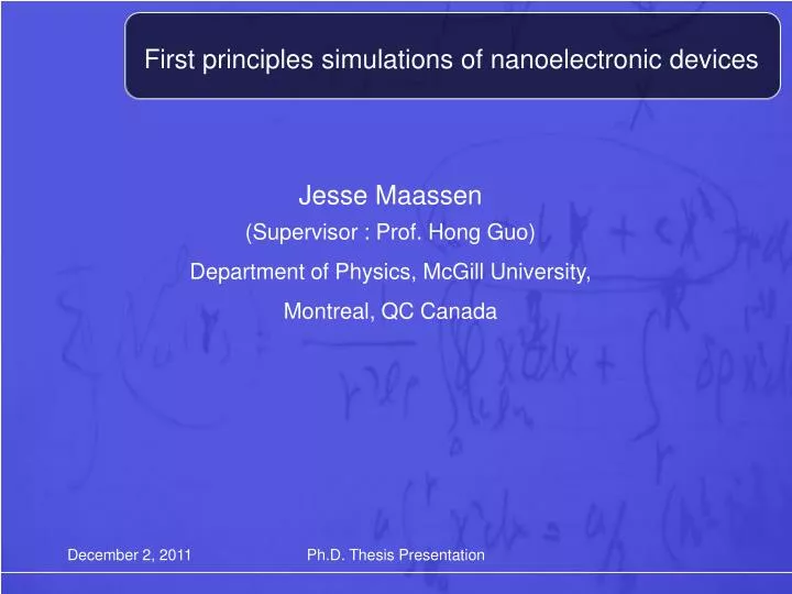
First principles simulations of nanoelectronic devices. Jesse Maassen (Supervisor : Prof. Hong Guo) Department of Physics, McGill University, Montreal, QC Canada. Year. Channel length. 2012. 22 nm. 2015. 16 nm. 2018. 11 nm ?. (Source: ITRS 2010). Line of ~ 50 atoms.

E N D
First principles simulations of nanoelectronic devices Jesse Maassen (Supervisor : Prof. Hong Guo) Department of Physics, McGill University, Montreal, QC Canada Ph.D. Thesis Presentation
Year Channel length 2012 22 nm 2015 16 nm 2018 11 nm ? (Source: ITRS 2010) Line of ~ 50 atoms Why first principles theory? Ph.D. Thesis Presentation
Science Engineering Atomic structure : surfaces, chemical bonding, interfaces, dissimilar materials, charge transfer, roughness, variability, … First principles Quantum effects : tunneling, conductance quantization, spin-transport, … Why first principles theory? Ph.D. Thesis Presentation
How to calculate transport properties? Taylor et al., PRB 63, 245407 (2001) Waldron et al., PRL 97, 226802 (2006) Maassen et al., IEEE (submitted) Ph.D. Thesis Presentation
Applications. • Graphene-metal interface • Localized doping in Si nano-transistors • Dephasing in nano-scale systems Maassen et al., Appl. Phys. Lett. 97, 142105 (2010); Maassen et al., Nano. Lett. 11,151 (2011) Ph.D. Thesis Presentation
Applications. • Graphene-metal interface • Localized doping in Si nano-transistors • Dephasing in nano-scale systems Maassen and Guo, preprint to be submitted Ph.D. Thesis Presentation
Applications. • Graphene-metal interface • Localized doping in Si nano-transistors • Dephasing in nano-scale systems Maassen et al., PRB 80, 125423 (2009) Ph.D. Thesis Presentation
Applications. • Graphene-metal interface • Localized doping in Si nano-transistors • Dephasing in nano-scale systems Maassen et al., PRB 80, 125423 (2009) Ph.D. Thesis Presentation
Application : Graphene-metal interface • Graphene has interesting properties (i.e., 2D material, zero gap, linear dispersion bands, …). Motivation : • For electronics, all graphene sheets must be contacted via metal electrodes (source/drain). • Theoretical studies exclude accurate treatment of electrodes. • How does the graphene/metal interface affect the response of a device? Ph.D. Thesis Presentation
Application : Graphene-metal interface Transport properties : Ph.D. Thesis Presentation
Metal Metal eq Application : Graphene-metal interface Atomic structure : • Cu, Ni and Co (111) have in-place lattice constants that almost match that of graphene. • Equilibrium interface structure determined from atomic relaxations. Maassen et al., Appl. Phys. Lett. 97, 142105 (2010); Maassen et al., Nano. Lett. 11,151 (2011) Ph.D. Thesis Presentation
Application : Graphene-metal interface Ni(111) contact : • Linear dispersion bands near Fermi level. • Zero band gap. • States only in the vicinity of K. Ph.D. Thesis Presentation
: Top-site C(pz) : Hollow-site C(pz) : Ni(dZ2) Application : Graphene-metal interface Ni(111) contact : • Strong hybridization with metal • Band gap opening • Graphene is spin-polarized Ph.D. Thesis Presentation Maassen et al., Nano. Lett. 11, 151 (2011)
Maassen et al., Nano. Lett. 11, 151 (2011) Application : Graphene-metal interface Ni(111) contact : Ph.D. Thesis Presentation
Maassen et al., Nano. Lett. 11, 151 (2011) Application : Graphene-metal interface Ni(111) contact : Ph.D. Thesis Presentation
CHANNEL Application : Localized doping in Si nano-transistors Motivation : • Leakage current accounts for 60% of energy in transistors. • Two sources : (i) gate tunneling and (ii) source/drain tunneling. • How can highly controlled doping profiles affect leakage current ? Ph.D. Thesis Presentation
Application : Localized doping in Si nano-transistors • Structure: n-p-n and p-n-p. • Channel doping: B or P. • L = 6.5 nm 15.2 nm • Si band gap = 1.11 eV Technical details regarding random doping, large-scale modeling and predicting accurate semiconductor band gaps can be found in the thesis. Ph.D. Thesis Presentation
Application : Localized doping in Si nano-transistors • GMAX / GMIN ~ 50. • Lowest G with doping in the middle of the channel. Maassen and Guo, preprint to be submitted Ph.D. Thesis Presentation
Application : Localized doping in Si nano-transistors Maassen and Guo, preprint to be submitted Ph.D. Thesis Presentation
Application : Localized doping in Si nano-transistors Maassen and Guo, preprint to be submitted Ph.D. Thesis Presentation
Application : Localized doping in Si nano-transistors • G decreases with L. • Variations in G increase dramatically with L. Maassen and Guo, preprint to be submitted Ph.D. Thesis Presentation
Application : Localized doping in Si nano-transistors • G decreases with L. • Variations in G increase dramatically with L. Maassen and Guo, preprint to be submitted Ph.D. Thesis Presentation
Summary • First principles transport theory is a valuable tool for quantitative predictions of nanoelectronics, where atomic/quantum effects are important. • I determined that the effect of metallic contacts (Cu, Ni, Co) can significantly influence device characteristics. I found that the atomic structure of the graphene/metal interface is crucial for a accurate treatment. • My simulations on localized doping profiles demonstrated how leakage current can be substantially reduced in addition to alleviating device variations. Ph.D. Thesis Presentation
Thank you! Questions ? Ph.D. Thesis Presentation