Download
1 / 24
250 likes | 405 Views
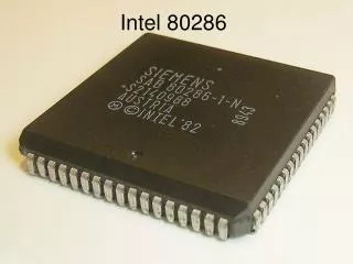
Chapter 2 80286 Microprocessor and Supporting Chips Section 2.1 80286 Microprocessor 1. 68 pins 2. LCC (leaded chip carrier) or PGA (pin grid array) package 3. Real mode or Protected mode 4. Power on real mode 5. Power off to leave protected mode. Pin Descriptions

E N D
Chapter 2 80286 Microprocessor and Supporting Chips Section 2.1 80286 Microprocessor 1. 68 pins 2. LCC (leaded chip carrier) or PGA (pin grid array) package 3. Real mode or Protected mode 4. Power on real mode 5. Power off to leave protected mode
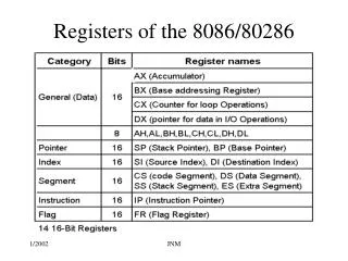
Pin Descriptions Pins A0~A23 (Address Bus) Pins D0~D15 (Data Bus) Pin BHE (Bus High Enable)
Pin CLK (clock) • Internal frequency = CLK/2 Pin M/IO (memory I/O select) Pin COD/INTA (code/interrupt acknowledge) Pins S1 and S0 (status signals)
Pins HOLD and HLDA (hold and hold acknowledge) 1. HOLD is used for DMA to request permission to use the buses. 2. HLDA: Hold acknowledge RESET pin 1. It stays high for at least 16 clocks. 2. A20=1, A21=1, A22=1, A23=1 3. As long as the RESET pin is high, no instruction or bus activity is allowed. 4. Enter into real mode
Pin INTR (interrupt request) expansion along with the 8259 interrupt controller chip Pin NMI (nonmaskable interrupt request) When this pin is activated, the 80286 will automatically perform INT 2. READY pin to insert a wait state for slow memory or I/O devices PEREQ and PEACK (processor extension request and acknowledge) used with the math processor 80287
BUSY pin Busy is an active-low input signal used by the math coprocessor to inform the 286 that it should stop program execution on WAIT and some ESC instruction. ERROR pin used by the math coprocessor INT 16 Vss pin Vcc pin CAP pin A 0.047F capacitor (with 20%, 12V) must be connected between this pin and ground.
Section 2.2 82284 Clock Generator • 82284 and 8284 are not interchangeable Pin description Pin F/C (frequency/crystal) Pin X1 and X2 The frequency of the crystal must be twice the desired frequency of the system. Pin EFI (external frequency in)
Pin CLK (clock) The 80286 system will work on one-half of whatever frequency is assigned to CLK. Pin PCLK (peripheral clock) a 50% duty cycleclock generator. It has a frequency one-half that of the crystal or one-half of CLK. Pins S0, S1 (status signal) They are used for synchronization of PCLK and READY. Pin RES (reset)
Pin RESET Pins SRDY (sync. ready) and SRDYEN (sync. ready enable) Pins ASRDY (async. Ready) and ASRDYEN (asynch. Ready enable) Pin READY Pins Vcc (power) and GND (ground)
Pin CLK (clock) Pins M/IO, S0, and S1 Pin READY Pins MB (multi bus mode) and CEN/AEN (command/address enable) Pass control of the system bus between the 80286 and DMA. Pin CMDLY (command delay) used along with READY to prolong the memory and I/O cycle time of the 80286. Pin CENL (command enable latch) connected to Vcc when there is onlt one 82288 bus controller in the system.
Pin ALE (address latch enable) due to the need for stable addresses in any system, ALE is used in the 80286 to latch the address into a 74XX373 latch. Pins IOWC, IORC, MWTC, MRDC Pin INTA (interrupt acknowledge) Pin DT/R (data transfer/receive) Pin DEN (data enable) for isolating the system data bus from the local data bus (for 74XX245) Pin MCE (master cascade enable) used with the 8259 interrupt controller chip to expand the number of hardware interrupts Pins Vcc (power) and GND (ground)
Section 2.4 80286 in IBM PC AT and ISA Buses IBM PC AT often refers to as ISA (Industry Standard Architecture) bus computers. 80286 and the origin of the ISA Buses The first IBM PC AT used 80286 82288 82284 74ALS 245 (transceiver) , 74ALS573 (address latch), 74ALS244 (unidirectional bus buffer), Shown in Fig. 2-4.
Address Bus Address bus A0-A19 is latched by 74ALS573 using the ALE signal. A20 Gate and the case of high memory area (HMA) A20 is gated into circuitry to allow it to overcome an anomaly associated with 286 and higher microprocessors. In 8086: +1 FFFFF 00000 In 80286 or higher +1 FFFFF 100000 instead of 00000 Here A20=1, How to solve it?
Data Bus The data bus is composed of pins D0 to D15. The data bus is buffered by a pair of 74ALS245 data bus transceivers.