Download
1 / 38
390 likes | 463 Views
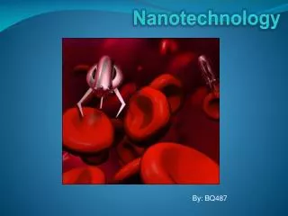
Nanotechnology: A Job for Many Markets. NCPN Conference Atlanta 2009 Deb Newberry By Tuesday, 6 October – this presentation can be found at dctc.edu – program and courses – nanoscience technician. “nano”. The prefix “nano” comes from the Greek word that means one billionth

E N D
Nanotechnology: A Job for Many Markets NCPN Conference Atlanta 2009 Deb Newberry By Tuesday, 6 October – this presentation can be found at dctc.edu – program and courses – nanoscience technician
“nano” • The prefix “nano” comes from the Greek word that means one billionth • When the prefix “nano” is applied to a length, like a meter we have • One billionth of a meter or 10 -9 m • Or one nanometer (nm) • Atoms are smaller than 1 nm, One hydrogen atom is about 1/10 of a nm. Gold atoms are a bit smaller than ½ of a nm. • DNA is about 2.5 nm across • And a human hair is about 100,000 nm in diameter (not length) • Molecules are formed by individual atoms that have interactions over a range of a few to tens of nanometers
Nanotechnology is….. the ability to observe, image, study, measure and manipulate at the molecular and atomic scale.
Over the last several decades… Modifications Improvements New ‘scopes
Atomic (electronic) structure Why is understanding the molecular or atomic level structure of a material important? Molecular structure Physical characteristics Electrical characteristics Biological characteristics
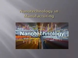
About Nanotechnology • Nanotechnology – Application of specific tools (Atomic Force Microscopes, Scanning Electron Microscopes etc.) that allow us to observe and manipulate material at the molecular or atomic scale. • Over 700 products currently in the market which take advantage of nanotechnology. • Every industry or market segment will be impacted by nanotechnology, with impacts in electronics and material science applications coming first, communication and disease diagnostic applications in the near future and in vivo disease treatment approaches or tailored drugs in the far future. • The application of nanoscience to industry is forecasted to create billions of dollars of revenue over the next 10 to 15 years. • Need for trained employees is critical to support the anticipated economic growth. Over 800,000 trained employees needed in the next 10 years in the US with over 50% being technicians. (Estimate is 4 to 6 technicians per PhD researcher.)
The Connection • Nanotech is global • Nanotechnology will impact every market segment • Nanotechnology will be a part of many careers • Challenge and Opportunity in Education
The Connection • Nanotech is global • Nanotechnology will impact every market segment • Nanotechnology will be a part of many careers • Challenge and Opportunity in Education
2004 On a typicaldaysomewhere in Europe …. On a typical day in Europe …..
Cosmetics TiO2 Nanoparticle Air Bag Accelaration Sensors MEMS GPS Navigation Functional Materials Pace Maker Li-Batteries New Materials for Energy Artificial Hips Biocompatible Materials Glasses and Coatings Optical Materials UV Filter Mobile Phone SAW Structures Digital Camera CCD Chip Artificial Lens Biocompatible Polymers Exact Time via satellite Semiconductíng devices Micro-Batteries Intelligent Credit Card Integrated Circuits Bike Frame Carbon Fibres Composite Materials GMR Read Head Magnetic Multilayers LED Display Photonic Materials Catalyzer Nanoparticles Taylored Materials at Work ….
The Connection • Nanotech is global • Nanotechnology will impact every market segment • Nanotechnology will be a part of many careers • Challenge and Opportunity in Education
Material Science Engineering Physics NanoScience Nanotechnology Chemistry Medicine Biology
Hysitron Nanomechnaical • measurement systems • Measurement and Analysis • Fabrication and Manufacturing • Biological • Ceramics • Composites • MEMS testing • Metals • Polymers • Thin films Scanning Electron Microscope (SEM) X-ray Diffractometer
Sample indents on metal • Nickel on Silicon • Oxidized Aluminum Scanning Electron Microscope (SEM) X-ray Diffractometer
Quality Control Systems Technician Mechanical Design and Engineering Physics Quality Control • Component testing • System testing • Tip testing • Interact with • R & D • Production • Software Development • Nanomechanics Research Laboratory • Customer Service and Sales Scanning Electron Microscope (SEM) X-ray Diffractometer
Chemistry or Nanotechnology or BOTH? Surface Properties Scanning Electron Microscope (SEM) X-ray Diffractometer
Material Science or Nanotechnology Or BOTH? Surface Properties Scanning Electron Microscope (SEM) X-ray Diffractometer
Examples of Multi-disciplinary Nanotechnology Scanning Electron Microscope (SEM) X-ray Diffractometer
Applicable Jobs • Medical Laboratory Technician • Research Team Member/ Assistant • Chemical Lab Tech • Jack of All trades • Test Technician • QA, Metrology Engineer/Technician • Graphics • Computer Simulation • Marketing • Business Development
Many Facets of Needed Nanotech Skills • Manufacturing (Exponential influence of nano) • Process Engineering and Development • Safety • Metrology • QA, reliability • Electronics • Processing • Process monitoring and test • Research
The expansion and “morphing” of nanotechnology • Expansion: • More companies are becoming aware of the advantages and necessity of understanding their product at the nanoscale • Result: installation of nanotechnology “scopes” • Electronics, drugs, medical devices, batteries, coatings, lubricants, foods, lotions, inks – an example: shingle material • This requires a combination of the specific industry discipline or SKAs and the ability and knowledge of nanotechnology and the equipment • Morphing: • Over the next 5 years nanoscience will move from the research lab to manufacturing of products using nanotechnology • Requires traditional process engineering, production design, quality assurance, metrology, reliability expertise to be coupled with a degree of nanotechnology awareness
Multiple paths to almost the same set of skills ( = or < 2 yr degree) • “Expert” nano (concept, application, practice)/ Proficient in other • “Expert” in other/ (high) proficiency in nano • “Expert” in other/ (high) proficiency in specific nano area or tool • Certificates for incumbent workers or other program grads • Retraining/skill enhancement for workers • How do you choose? • 1) Look at what you/your school/ region are good at • 2) Go to the local and regional industries • This will require work on your part – can’t have a blank sheet of paper • Local chapters of professional organizations (IEEE, ACS, ASME etc.)
Ah! – but here’s the “rub”Industry Perspective – with a “nano” slant • Want not only “skilled’ workers but “ knowledgeable” workers • Understanding of “skilled “ workers exists • Understanding of “knowledgeable” does not • What does “knowledgeable” mean? • Knowledgeable can have many degrees or steps • Concept of the nanoscale, equipment operation, data analysis • How to differentiate different skill levels • This is a real problem that needs to be worked • Matching with industry needs
Admin Other faculty Guide Nano “Idea” Industry Patience State
I have all the support and know the direction I want to go • No • Talk to a guide/consultant • NACK (Penn State) – multi-disciplinary AAS (with articulation) • Semester 4 • Educator Training • DCTC/Nano-Link – multi-disciplinary AAS (with articulation) • Semesters 1 – 4 • Educator Training U of MN • Other NSF Centers • Local NSF projects (NSF.gov) • Yes!!!! But don’t recreate the wheel • NACK – Complete Courses – 4th semester – on-line now • Nano-Link, Educational Content in self contained modular format – in process….nanomaterials modules by the end of the year. • Need more basic content? Contact Deb Newberry
Final words • Read “nano” stuff related to your field • Nature, Science, NanoToday, MaterialToday, NanoLetters, MIT technology Review, Scientific American • Get to know industry people – you will be surprised what 1 visit to a Rotary Club or Chamber of Commerce meeting can do • Plan your approach • Line up your support network • Thank you!!!!! • dmnewberry2001@yahoo.com