Download
1 / 10
100 likes | 233 Views
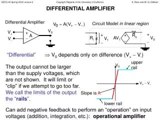
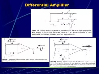
2.4 差動増幅回路 differential amplifier circuit. ï¼’ã¤ã®å…¥åŠ› 電圧ã®å·®ã‚’増幅 ã™ã‚‹å›žè·¯ã€‚ 温度や電æºé›»åœ§ãªã©ã®å¤‰å‹•ã®å½±éŸ¿ã‚’å—ã‘ã«ãã,åŒç›¸é›‘音を除去ã™ã‚‹ã®ã§ï¼Œã‚»ãƒ³ã‚µå›žè·¯ï¼Œè¨ˆæ¸¬å›žè·¯ç‰ã«åˆ©ç”¨ã•ã‚Œã‚‹ã€‚. 1.基本的ãªå›žè·¯. 定電æµãƒã‚¤ã‚¢ã‚¹å›žè·¯. åŒç›¸ã‚²ã‚¤ãƒ³ã®ï¼¡ï¼£è§£æžçµæžœ. Output No.1,No2 ã¨ã‚‚ã«åŒã˜. ä½ç›¸. ゲイン. 低域ã®åŒç›¸ã‚²ã‚¤ãƒ³ã¯ ç´„ï¼ï¼—2dB. 差動ゲインã®ï¼¡ï¼£è§£æž. Output No.1,No2 ã¨ã‚‚ã«åŒã˜. ä½ç›¸. ゲイン. 一方ã®ç¬¦å·ã‚’逆転ã™ã‚‹. 差動ゲインã®ï¼¡ï¼£è§£æžçµæžœ.

E N D
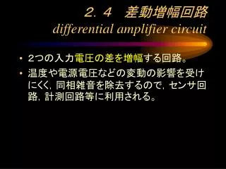
2.4 差動増幅回路differential amplifier circuit • 2つの入力電圧の差を増幅する回路。 • 温度や電源電圧などの変動の影響を受けにくく,同相雑音を除去するので,センサ回路,計測回路等に利用される。
1.基本的な回路 定電流バイアス回路
同相ゲインのAC解析結果 Output No.1,No2ともに同じ 位相 ゲイン 低域の同相ゲインは約-72dB
差動ゲインのAC解析 Output No.1,No2ともに同じ 位相 ゲイン 一方の符号を逆転する
差動ゲインのAC解析結果 Output No.1,No2ともに同じ Output No.1の位相 Output No.1,No. 2のゲイン Output No. 2の位相 低域のゲインは約31dB
同相信号除去比(CMRR : Common Mode Rejection Ratio) [定義] CMMR= 20 log10(CVD / CVN) = 20 log10 CVD - 20 log10 CVN ただし,CVD:差動電圧増幅率, CVN:差動電圧増幅率である。 ゲインをそれぞれGVD,GVNとすると,デシベルの定義から CMMR =GVD-GVN 解析結果から, CMMR=31.157-(-72.395)=103.552
2.定電流バイアス回路を抵抗で置き換える 定電流バイアス回路を抵抗で置き換える
AC解析結果 同相ゲイン -6.7267 差動ゲイン 31.153 CMRR : 31.153-(-6.727)=37.880(定電流バイアス回路を使う場合に103.552に比べて悪い)
3.定電流バイアス回路をカレント・ミラー回路で置き換える3.定電流バイアス回路をカレント・ミラー回路で置き換える カレントミラー回路
AC解析結果 同相ゲイン -27.881 差動ゲイン 31.185 CMRR : 31.185-(-27.881)=59.066宿題 : カレントミラー回路をウィルソン型などに変えてみよう