Download
1 / 46
460 likes | 603 Views
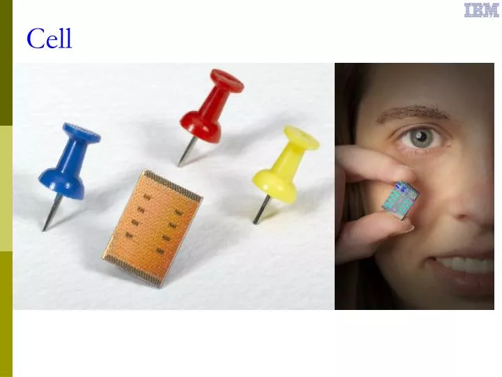
Systems and Technology Group. Cell. Introduction to the Cell Broadband Engine Architecture. A new class of multicore processors being brought to the consumer and business market.

E N D
Introduction to the Cell Broadband Engine Architecture • A new class of multicore processors being brought to the consumer and business market. • A radically different design which warrants a brief discussion of the Cell/B.E. hardware and software architecture.
Cell Broadband Engineoverview • The result of a collaboration between Sony, Toshiba, and IBM (known as STI), which formally began in early 2001. • Initially intended for applications in media-rich consumer-electronics devices (game consoles, high-definition TV), designed to enable fundamental advances in processor performance. • These advances are expected to support a broad range of applications in both commercial and scientific fields.
Scaling the three performance-limiting walls • Power wall • Frequency wall • Memory wall
Scaling the power-limitation wall • Microprocessor performance is limited by achievable power dissipation rather than by the number of available integrated-circuit resources • Need to improve power efficiency at about the same rate as the performance increase. • One way to increase power efficiency is to differentiate between the following types of processors: • Processors that are optimized to run an operating system and control-intensive code • Processors that are optimized to run compute-intensive applications
Scaling the power-limitation wall • A general-purpose core to run the operating system and other control-plane code. Eight coprocessors specialized for computing data-rich (data-plane) applications. • The specialized coprocessors are more compute efficient because they have simpler hardware implementations (no branch prediction, out-of-order execution, speculation, etc..) • By weight, more of the transistors are used for computation than in conventional processor cores.
Scaling the frequency-limitation wall • Conventional processors require increasingly deeper instruction pipelines to achieve higher operating frequencies. • This technique has reached a point of diminishing returns, and even negative returns if power is taken into account. • By specializing the GP-core and the coprocessors for control and compute-intensive tasks, respectively, the Cell/B.E. allows both them to be designed for high frequency without excessive overhead.
Scaling the frequency-limitation wall • GP-core efficiency • two threads simultaneously rather than by optimizing single-thread performance. • Coprocessor efficiency • Large register file, which supports many simultaneous in-process instructions without the overhead of register-renaming or out-of-order processing. • Asynchronous DMA transfers, which support many concurrent memory operations without the overhead of speculation.
Scaling the memory-limitation wall • On multiprocessors (SMPs) latency to DRAM memory is currently approaching 1,000 cycles. • Execution time is dominated by data movement between main storage and the processor. • Compilers and applications must manage this movement of data explicitly (to aid hardware cache mechanisms)
Scaling the memory-limitation wall • The Cell/B.E. processor use two mechanisms to deal with long main-memory latencies: • Three-level memory structure • Asynchronous DMA transfers • These features allow programmers to schedule simultaneous data and code transfers to cover long latencies effectively. • Because of this organization, the Cell/B.E. processor can usefully support 128 simultaneous transfers. • This surpasses the number of simultaneous transfers on conventional processors by a factor of almost twenty.
How the Cell/B.E. processor overcomes performance limitations • By optimizing control-plane and data-plane processors individually, the Cell/B.E. processor alleviates the problems posed by power, memory, and frequency limitations. • The net result is a processor that, at the power budget of a conventional PC processor, can provide approximately ten-fold the peak performance of a conventional processor. • Actual application performance varies. • Some applications may benefit little from the SPEs, where others show a performance increase well in excess of ten-fold. • In general, compute-intensive applications that use 32-bit or smaller data formats, such as single-precision floating-point and integer, are excellent candidates for the Cell/B.E. processor.
SPU SPU SPU SPU SPU SPU SPU SPU SXU SXU SXU SXU SXU SXU SXU SXU LS LS LS LS LS LS LS LS MFC MFC MFC MFC MFC MFC MFC MFC PPU L1 PXU 16B/cycle Cell System Features • Heterogeneous multi-core system architecture • Power Processor Element for control tasks • Synergistic Processor Elements for data-intensive processing • Synergistic Processor Element (SPE) consists of • Synergistic Processor Unit (SPU) • Synergistic Memory Flow Control (MFC) • Data movement and synchronization • Interface to high-performance Element Interconnect Bus SPE 16B/cycle EIB (up to 96B/cycle) 16B/cycle 16B/cycle 16B/cycle (2x) PPE MIC BIC L2 32B/cycle Dual XDRTM FlexIOTM 64-bit Power Architecture with VMX
Cell Broadband Engine TM:A Heterogeneous Multi-core Architecture * Cell Broadband Engine is a trademark of Sony Computer Entertainment, Inc.
PPU Organization • Power Processor Element (PPE): • General Purpose, 64-bit RISC Processor (PowerPC 2.02) • 2-Way Hardware Multithreaded • L1 : 32KB I ; 32KB D • L2 : 512KB • VMX (Vector Multimedia Extension) • 3.2 GHz
8 SPEs-128-bit SIMD instruction set- Local store – 256KB- MFC
SPE Organization • Local Store is a private memory for program and data • Channel Unit is a message passing I/O interface • SPU programs DMA Unit with Channel Instructions • DMA transfers data between Local Store and system memory
SIMD Architecture • SIMD = “single-instruction multiple-data” • SIMD exploits data-level parallelism • a single instruction can apply the same operation to multiple data elements in parallel • SIMD units employ “vector registers” • each register holds multiple data elements • SIMD is pervasive in the BE • PPE includes VMX (SIMD extensions to PPC architecture) • SPE is a native SIMD architecture (VMX-like)
A SIMD Instruction Example • Example is a 4-wide add • each of the 4 elements in reg VA is added to the corresponding element in reg VB • the 4 results are placed in the appropriate slots in reg VC
Local Store • Never misses • No tags, backing store, or prefetch engine • Predictable real-time behavior • Less wasted bandwidth • Software managed caching • Can move data from one local store to another
DMA & Multibuffering • DMA commands move data between system memory & Local Storage • DMA commands are processed in parallel with software execution • Double buffering • Software Multithreading • 16 queued commands
Element Interconnect Bus - Data Topology • Four 16B data rings connecting 12 bus elements • Physically overlaps all processor elements • Central arbiter supports up to 3 concurrent transfers per data ring • Each element port simultaneously supports 16B in and 16B out data path • Ring topology is transparent to element data interface SPE1 SPE3 SPE5 SPE7 PPE IOIF1 16B 16B 16B 16B 16B 16B 16B 16B 16B 16B 16B 16B Data Arb 16B 16B 16B 16B 16B 16B 16B 16B 16B 16B 16B 16B BIF/IOIF0 SPE6 MIC SPE0 SPE2 SPE4
MIC PPE SPE0 SPE1 SPE2 SPE3 SPE4 SPE5 SPE6 SPE7 BIF / IOIF1 PPE PPE MIC SPE3 SPE5 SPE0 SPE2 SPE4 SPE6 IOIF1 SPE1 SPE5 SPE3 IOIF1 SPE1 SPE7 SPE7 Ramp 11 Ramp 10 Ramp 7 Ramp 8 Ramp 9 Ramp 6 Controller Controller Controller Controller Controller Controller Controller Ramp 4 Controller Ramp 0 Controller Ramp 1 Controller Ramp 2 Controller Ramp 5 Controller Ramp 3 BIF / IOIF1 Example of eight concurrent transactions Ramp 7 Controller Ramp 8 Controller Ramp 9 Controller Ramp 10 Controller Ramp 11 Controller Data Arbiter Ramp 7 Controller Ramp 8 Controller Ramp 9 Controller Ramp 10 Controller Ramp 11 Controller Controller Controller Controller Controller Controller Controller Ramp 5 Ramp 4 Ramp 3 Ramp 2 Ramp 1 Ramp 0 IOIF0 Ring1 Ring0 controls Ring3 Ring2
IBM SDK for Multicore Acceleration • Compilers • IBM Full System Simulator • Linux kernel • Cell/B.E. libraries • Code examples and example libraries • Performance tools • IBM Eclipse IDE for the SDK
Compilers • GNU toolchain • The GNU toolchain, including compilers, the assembler, the linker, and miscellaneous tools, is available for both the PowerPC Processor Unit (PPU) and Synergistic Processor Unit (SPU) instruction set architectures. • On the PPU, it replaces the native GNU toolchain, which is generic for the PowerPC Architecture, with a version that is tuned for the Cell/B.E. PPU processor core. • The GNU compilers are the default compilers for the SDK. • The GNU toolchains run natively on Cell/B.E. hardware or as cross-compilers on PowerPC or x86 machines. • IBM XLC/C++ compiler • IBM XL C/C++ for Multicore Acceleration for Linux is an advanced, high-performance cross-compiler that is tuned for the Cell Broadband Engine Architecture (CBEA). • The XL C/C++ compiler generates code for the PPU or SPU. • The compiler requires the GCC toolchain for the CBEA, which provides tools for cross-assembling and cross-linking applications for both the PowerPC Processor Element (PPE) and Synergistic Processor Element (SPE). • OpenMP compiler: The IBM XLC/C++ compiler that comes with SDK 3 is an OpenMP directed single source compiler that supports automatic program partitioning, data virtualization, code overlay, and more. This version of the compiler is in beta mode. Therefore, users should not base production applications on this compiler.
IBM Full System Simulator • The IBM Full System Simulator is a software application that emulates the behavior of a full system that contains a Cell/B.E. processor. • You can start a Linux operating system on the simulator, simulate a two chip Cell/B.E. environment, and run applications on the simulated operating system. • The simulator also supports the loading and running of statically-linked executable programs and stand-alone tests without an underlying operating system. • The simulator infrastructure is designed for modeling the processor and system-level architecture at levels of abstraction, which vary from functional to performance simulation models with several hybrid fidelity points in between: • Functional-only simulation • Performance simulation • The simulator for the Cell/B.E. processor provides a cycle-accurate SPU core model that can be used for performance analysis of computationally-intense applications.
Cell/B.E. libraries • SPE Runtime Management Library • SIMD Math Library • Mathematical Acceleration Subsystem libraries • Basic Linear Algebra Subprograms • ALF library • Data Communication and Synchronization library
Performance tools • SPU timing tool • OProfile • Cell-perf-counter tool • Performance Debug Tool • Feedback Directed Program Restructuring tool • Visual Performance Analyzer
IBM Eclipse IDE for the SDK • IBM Eclipse IDE for the SDK is built upon the Eclipse and C Development Tools (CDT) platform. It integrates the GNU toolchain, compilers, the Full System Simulator, and other development components to provide a comprehensive, Eclipse-based development platform that simplifies development. • Eclipse IDE for the SDK includes the following key features: • A C/C++ editor that supports syntax highlighting, a customizable template, and an outline window view for procedures, variables, declarations, and functions that appear in source code • A visual interface for the PPE and SPE combined GDB (GNU debugger) and seamless integration of the simulator into Eclipse Automatic builder, performance tools, and several other enhancements; remote launching, running and debugging on a BladeCenter QS21; and ALF source code templates for programming models within IDE • An ALF Code Generator to produce an ALF template package with C source code and a readme.txt file • A configuration option for both the Local Simulator and Remote Simulator target environments so that you can choose between launching a simulation machine with the Cell/B.E. processor or an enhanced CBEA-compliant processor with a fully pipelined, double precision SPE processor • Remote Cell/B.E. and simulator BladeCenter support • SPU timing integration and automatic makefile generation for both GCC and XLC projects
CELL Software Design Considerations • Two Levels of Parallelism • Regular vector data that is SIMD-able • Independent tasks that may be executed in parallel • Computational • SIMD engines on 8 SPEs and 1 PPE • Parallel sequence to be distributed over 8 SPE / 1 PPE • 256KB local store per SPE usage (data + code) • Communicational • DMA and Bus bandwidth • DMA granularity – 128 bytes • DMA bandwidth among LS and System memory • Traffic control • Exploit computational complexity and data locality to lower data traffic requirement
Determining whether the Cell/B.E. system fits the application requirements
Typical CELL Software Development Flow • Algorithm complexity study • Data layout/locality and Data flow analysis • Experimental partitioning and mapping of the algorithm and program structure to the architecture • Develop PPE Control, PPE Scalar code • Develop PPE Control, partitioned SPE scalar code • Communication, synchronization, latency handling • Transform SPE scalar code to SPE SIMD code • Re-balance the computation / data movement • Other optimization considerations • PPE SIMD, system bottle-neck, load balance • NOTES: Need to push all computational tasks to SPEs
Linux Kernel Support • PPE runs PowerPC applications and operating systems • PPE handles thread allocation and resource management among SPEs • PPE’s Linux kernel controls the SPUs’ execution of programs • Schedule SPE execution independent from regular Linux threads • Responsible for runtime loading, passing parameters to SPE programs, notification of SPE events and errors, and debugger support • PPE code – Linux tasks • a Linux task can initiate one or more “SPE threads” • SPE code – “local” SPE executables (“SPE threads”) • SPE executables are packaged inside PPE executable files • An SPE thread: • is initiated by a task running on the PPE • runs asynchronously from initiating task • has a unique identifier known to both the SPE thread and the initiating task
PPE vs SPE • Both PPE and SPE execute SIMD instructions • PPE processes SIMD operations in the VXU within its PPU • SPEs process SIMD operations in their SPU • Both processors execute different instruction sets • Programs written for the PPE and SPEs must be compiled by different compilers
Communication Between the PPE and SPEs • PPE communicates with SPEs through MMIO registers supported by the MFC of each SPE • Three primary communication mechanisms between the PPE and SPEs • Mailboxes • Queues for exchanging 32-bit messages • Two mailboxes are provided for sending messages from the SPE to the PPE • SPU Write Outbound Mailbox • SPU Write Outbound Interrupt Mailbox • One mailbox is provided for sending messages to the SPE • SPU Read Inbound Mailbox • Signal notification registers • Each SPE has two 32-bit signal-notification registers, each has a corresponding memory-mapped I/O (MMIO) register into which the signal-notification data is written by the sending processor • Signal-notification channels, or signals, are inbound (to an SPE) registers • They can be used by other SPEs, the PPE, or other devices to send information, such as a buffer-completion synchronization flag, to an SPE • DMAs • To transfer data between main storage and the LS
PPE and SPE MFC Command Differences • Code running on the SPU issues an MFC command by executing a series of writes and/or reads using channel instructions • Code running on the PPE or other devices issues an MFC command by performing a series of stores and/or loads to memory-mapped I/O (MMIO) registers in the MFC • Data-transfer direction for MFC DMA commands is always referenced from the perspective of an SPE • get: transfer data into an SPE (from main storage to local store) • put: transfer data out of an SPE (from local store to main storage)
Data Transfer Between Main Storage and LS Domain • An SPE or PPE performs data transfers between the SPE’s LS and main storage primarily using DMA transfers controlled by the MFC DMA controller for that SPE • Channels • Software on the SPE’s SPU interacts with the MFC through channels, which enqueue DMA commands and provide other facilities, such as mailboxes, signal notification, and access auxiliary resources • DMA transfer requests contain both an LSA and an EA • Thus, they can address both an SPE’s LS and main storage • Each MFC can maintain and process multiple in-progress DMA command requests and DMA transfers • Each DMA command is tagged with a 5-bit Tag Group ID. This identifier is used to check or wait on the completion of all queued commands in one or more tag groups
Uses of Mailboxes • To communicate messages up to 32 bits in length, such as buffer completion flags or program status • e.g., When the SPE places computational results in main storage via DMA. After requesting the DMA transfer, the SPE waits for the DMA transfer to complete and then writes to an outbound mailbox to notify the PPE that its computation is complete • Can be used for any short-data transfer purpose, such as sending of storage addresses, function parameters, command parameters, and state-machine parameters
Mailboxes - Characteristics Each MFC provides three mailbox queues of 32 bit each: • PPE (“SPU write outbound”) mailbox queue • SPE writes, PPE reads • 1 deep • SPE stalls writing to full mailbox • PPE (“SPU write outbound”) interrupt mailbox queue • like PPE mailbox queue, but an interrupt is posted to the PPE when the mailbox is written • SPU (“SPU read inbound”) mailbox queue • PPE writes, SPE reads • 4 deep • can be overwritten