Download
1 / 29
290 likes | 408 Views
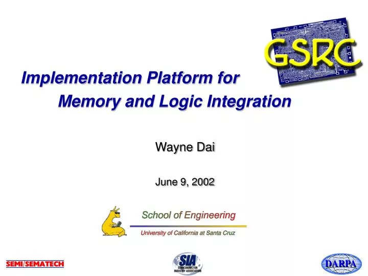
Implementation Platform for Memory and Logic Integration. Wayne Dai June 9, 2002. Outline. Challenges and opportunities for System-in-a-Package (SiP) SiP implementation platform for memory/logic integration Configurable area-IO memory architecture

E N D
Implementation Platform for Memory and Logic Integration Wayne Dai June 9, 2002
Outline • Challenges and opportunities for System-in-a-Package (SiP) • SiP implementation platform for memory/logic integration • Configurable area-IO memory architecture • SiP performance analysis and modeling based on GTX framework • Concluding remarks
Messages from ITRS • Package cost increases 5% each year. • 8% - 11% increase in pin count per packaged IC each year, 5% reduction in cost per pin each year. • Inter-chip signal integrity issues will be more challenging. • In 2002, chip to board clock frequency is 400MHz for cost-performance system, 800MHz for high-performance system. • Package size can not shrink due to the fanout problem. • Moore’s law is good for silicon, but not good for board. • System-on-a-Chip is not always a good idea. • Cost penalty, complexity of design and verification, difficulty of integrating different technologies…
Flash uP DRAM The Y Chart of System Design ARCHITECTURAL DOMAIN FUNCTIONAL DOMAIN Synthesis Implementation Missing • Platform-based design methodology is the only solution to deliver complex embedded systems in a limited design time. PHYSICAL DOMAIN uP Flash DRAM
System-in-a-Package Implementation Platform • A giant chip rather than a miniaturized circuit board: preserving on-chip electrical environment Chip-on-Chip DRAM and graphic chip integration Chip-Laminate-Chip
Characteristic: Maximum off-chip delay << IO buffer delay (3.5ns) Signal round trip time < rise time (500ps) Inter-chip skew < board skew (500ps) No terminating resistors required Smaller IO buffer size and minimized ESD protection Chip-Laminate-Chip Technology Logic side Memory side Laminate Logic Decoupling C BGA ball Area-IO DRAM Chip-Laminate-Chip (CLC) architecture Source: SyChip Inc.
CPU/North Bridge/Graphic Chip Integrated Core 500MHz DDR SDRAM CPU 700MHz L2 Cache (up to 2MB) North Bridge and Graphic Chip 266MHz DDR SDRAM Single-Package Computer • A high performance system • Server CPU (700MHz, 2MB L2 cache) • Graphic chip & north bridge • 266 MHz DDR SDRAM • The performance is limited by the memory access time • The power consumption of the CPU is over 30W in active mode • A low cost system • 500-700 MHz integrated core logic (integrated CPU, north bridge, and graphic chip) • 400-500 MHz DDR SDRAM • CLC BGA package • Better performance achieved by balancing the core logic and memory access speed
Issues Addressed… • What is the most cost-effective implementation platform for memory and logic integration, embedded DRAM, SiP, or PCB? What are the trade-offs? • What is the maximum bandwidth achievable by SiP? • What is the maximum IO speed? • How should the IO design take advantage of this platform? • How should the memory architecture be re-optimized for this platform?
…Issues Addressed • What is the routability of IO redistribution? • What will be the optimal power/ground structure on laminate? • What will be the optimal clock structure on laminate? • What is the model of junction temperature in SiP module? • Etc.
Outline • Challenges and opportunities for System-in-a-Package (SiP) • SiP implementation platform for memory/logic integration • Configurable area-IO memory architecture • SiP performance analysis and modeling based on GTX framework • Concluding remarks
IO Issues in System-in-a-Package • Integration with conventional logic and memory chips can not fully realize the potential of SiP
Logic&Buffer Logic&Buffer ESD Protection Circuit PAD PAD Area-IO Is the Solution! • Flip-chip technology preserves on-chip electrical environment for SiP. • ESD Protection can be minimized for intra-package IOs. • Design-specific IOs are desired for optimal driving strength. • Area-IO architecture provides rich power/ground pads for better signal integrity. Area-IO Conventional IO
Configurable Memory Architecture… • Different architectures require different memory organizations. Memory organization for n-bit-serial processors Memory organization for microprocessors Memory organization for graphics processors short word-width (1-8) large number of words large number of banks medium word-width (16-64) medium number of words multiple banks long word-width (512-1K) small number of words single bank
…Configurable Memory Architecture • Commercial memory can not provide high bandwidth communication with small chip/board area. • Embedded memory does not have the flexibility to change the memory organization for different programming models. • Configurable memory for System-in-a-Package (SiP) provides the opportunity to make one memory chip meet the requirements of different architectures. • Memory organization can be programmed for different architecture (n-bit-serial processors, microprocessors, graphics processors). • Word-width ranges from 8 to 1K.
Memory building block Memory building block Memory building block Memory building block Memory building block Memory building block Memory building block Memory building block Memory building block Memory building block Memory building block Memory building block Memory building block Memory building block Memory building block Memory building block Design Case: Configurable Area-IO SRAM • Give users the flexibility to program the memory for different applications. • 15 configuration modes. • Consists of 16 x 32k SRAMs with configuration control circuit. • Distributing area-IO cells all around the chip. • Easy to migrate to Multi-DRAM-Module. Area-IO Memory configuration logic
aSRAM Final Layout 3.85 mm 6.80 mm Top( 3.34M Tr., 570 Area-IO )
300 Peripheral-IO Area-IO 200 Number of Net 100 0 0.1 0.2 0.3 0.4 0.5 0.6 0.7 0.8 0.9 1.0 1.1 1.2 1.3 1.4 1.5 Capacitance (pF) Area-IO Vs. Peripheral-IO • Area-IO architecture significantly reduces the parasitic capacitance of IO redistribution. Area-IO rerouting Peripheral-IO rerouting
Outline • Challenges and opportunities for System-in-a-Package (SiP) • SiP implementation platform for memory/logic integration • Configurable area-IO memory architecture • SiP performance analysis and modeling based on GTX framework • Concluding remarks
DRAM Performance Analysis • Analyze DRAM delay/area/power based on architectural parameters (size, IO width, address width, etc.) and technological parameters (feature size, transistor size, cell capacitance, etc.) • Predict design feasibility based on SiP platform. • Compare different DRAM architectures and implementations. Enable designers to analyze the DRAM cost and performance without actual physical implementation.
Wordline Timing Wordline equivalent circuit Kbootstrap is a process dependent constant Wordline delay is proportional to wordline length.
Sense Amplifier Timing Sensing time Vs. bitline capacitance (SPICE simulation result) Ksenseamp is a process dependent constant Bitline delay is proportional to bitline capacitance.
DRAM Core Area Analysis • Compare core area of embedded DRAM and aDRAM for SiP. • aDRAM for SiP has area-IO architecture with various bit-width. • Assume ASIC technology for eDRAM and conventional DRAM technology for aDRAM. Area overhead of IO circuitry is not significant.
Implications from Our Study • DRAM performance can be improved by dividing DRAM cell array into smaller “self-contained” building blocks. • Additional IOs can be implemented with area array architecture. • With rich area-IO, it is possible to minimize or even remove column decoding circuit to improve timing. With SiP implementation platform, memory (DRAM/SRAM) architecture should be re-optimized for better electrical environment.
Routability Analysis for IO Rerouting • Given package size and number of pins, what ismaximum pin pitch? • Given number of pins, what is minimum package size? • Given package size, what is maximum total pins? Octilinear Routing All-Angle Routing
Planes Grid Mesh Planes Cross Traces Resistive drops Very low Low Medium Inductive drops Low Medium High # Layers High Medium Low Power/Ground Analysis for SiP… • How many P/G pins needed? • Where to place decoupling capacitors? On-chip? On-card? On-board? • How much decoupling capacitance? Too little noisy power supplies Too much unpredictable LC resonance increase die area Power/Ground Distribution Structure
…Power/Ground Analysis for SiP • On IC, hybrid full-wave techniques are applied for different types of P/G structures P/G Structure in Chip Field Computed with MEI Method • In package, EM fields are decomposed into two modes (J. Fang, UCSC) : • Strip-line mode fields propagate along metal traces • Parallel-plate mode field propagate between adjacent planes • Three to four orders of magnitude faster than ASTAP Signal Trace between Two Planes on Package Level A Pulse Propagate down the Via and onto the Trace
Thermal Analysis for SiP • Junction temperature should be estimated at early design stage. • Simplified thermal model can provide relatively accurate result for early analysis. • Detailed thermal simulation with numeric methods can be applied to obtain accurate junction temperature. Simplified thermal model for one logic, two DRAM SiP module
Concluding Remarks • System-on-a-Chip should be generalized to System-in-a-Package (SiP). • SiP provides new opportunities for gigascale integration. • SiP brings cost-effective alternatives for embedded DRAM. • Area-IO opens up a new paradigm for trading off on-chip interconnect versus on-package interconnect. • Configurable memory enables single memory chip to meet the requirements for various applications. • Cost/performance and design feasibility early analysis is highly desired for SiP implementation platform.