Download
1 / 31
320 likes | 432 Views
Reducing ATE Test Time BY Voltage and Frequency SCALING. By Praveen Venkataramani Committ e e Prof. Vishwani D. Agrawal (Advisor) Prof. Adit D. Singh Prof. Fa Foster Dai. Agenda. Background Problem statement Prior work A test time theorem Test time reduction methods Summary

E N D
Reducing ATE Test Time BY Voltage and Frequency SCALING By Praveen Venkataramani Committee Prof. Vishwani D. Agrawal (Advisor) Prof. Adit D. Singh Prof. Fa Foster Dai General Oral Exam
Agenda Background Problem statement Prior work A test time theorem Test time reduction methods Summary Future work General Oral Exam
TEST General Oral Exam
Background: methods of testing General Oral Exam • Testing can be perform using • Built In Self Test (BIST) • Circuit tests itself. • Contains test pattern generator and output response analyzer. • Test per scan or Test per clock • External Test – Automated Test Equipment, Bench Test. • Patterns are applied externally to the circuit under test. • Circuit response is captured and analyzed externally
Background: Scan Test • Sequential devices are hard to test. • Sequential devices are tested as combinational circuits by inserting scan flip flops. • Scan test consists of a shift mode and a capture mode. Combinational logic PO PI SO DFF DFF SI SE General Oral Exam
Background: Scan test procedure General Oral Exam Test pattern is shifted serially, setting scan enable (SE) high, through the scan flip flops during scan shift. Circuit is configured to capture by setting SE to low for one cycle. Captured response is shifted out in the next cycle Number of scan shift cycles depends on the length of the scan chain Each flip flop may toggle during scan shift and capture.
Problem Statement Power consumption during test must not exceed the specified budget often implying increased test time. Long test time increases cost; test time can be very long for scan based testing. Need to reduce test time without exceeding power budget. General Oral Exam
Prior Work Pattern overlapping - Reduce unwanted scan operations by using similar patterns. [Chloupek’12] Reusable scan chains - Unwanted scan shifts are avoided. [Lai’93] Activity monitor in BIST circuits - Monitor the activity in the vector from LFSR to manipulate the clock period dynamically. [Shanmugasundaram’12] Employing both BIST and ATE - Use BIST for easy-to-detect faults and then the ATE to identify the hard-to-detect faults. [Hashempour’02] Simultaneous testing – Twoor more cores are tested in parallel. [Zhao’03] General Oral Exam
Test Time • During scan shift/capture all flip flops may toggle. • Increase power dissipation during test. • Test time is affected by the number of patterns, the size of the scan chain and slow test clock frequency. • Rated power limits the maximum test clock frequency Combinational logic PO PI SO DFF DFF SI SE General Oral Exam
Test Time - Theorem The test time (TT) for a synchronous test is the ratio of total energy dissipated in the entire test to the average power consumption during test. Quantitatively this can be written as Where ETOTAL is the total energy, an invariant of the test, PAVG is the average power. General Oral Exam
Power Metrics [Patrick’10] General Oral Exam Energy: Energy is estimated as the total switching activity generated during test application. Power: Defined for a clock cycle is the energy dissipated divided by the clock period. Average Power: It is the average of power over the entire test. Maximum Power: It is the maximum power dissipated in any clock cycle during the entire test.
Observations Dynamic energy is not consumed evenly throughout the entire test. Reducing the voltage reduces power. Power dissipated is dependent on the clock period. General Oral Exam
Test Time Reduction • To reduce test time we can • Scale the supply voltage, increase the frequency to maintain the power dissipation. • Dissipate the energy at varying rate to maintain the same power dissipation. • Implement scaled supply voltage and varying rate. • Clock period is constrained • Structure: The period of the clock must not be shorter than the delay of the critical path. • Power: The period of the clock must not let the power dissipation exceed the design specification. General Oral Exam
Scaling Supply Voltage • Conventional method to perform test uses synchronous clock, i.e., uses fixed clock period • Test produces more signal transitions than functional operation, thus dissipate more power than the circuit is designed for. • The rated power determines the test clock period. • Effects of reducing voltage • Test power reduces • Critical path slows down General Oral Exam
Scaling Supply Voltage General Oral Exam
Scaling Supply Voltage - Results General Oral Exam
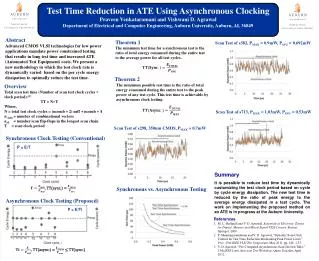
Varying Clock Period General Oral Exam In a synchronous test each period depends on the maximum power dissipated. Each period may not dissipate same amount of power. Periods can be varied based on the power dissipated. This is achieved by asynchronous test.
Varying Clock Period General Oral Exam • Each period in an asynchronous test can be either structure constrained or power constrained where Ti is the period of each test cycle Ei is the energy dissipated by each cycle • For any voltage an asynchronous test can run faster than the synchronous test at that voltage
Asynchronous Clock – s298 Example General Oral Exam
Asynchronous test on ATE General Oral Exam • Experimental Setup • The test was implemented on the Advantest T2000GS ATE at Auburn University. • Maximum clock speed of 250 MHz • CUT is an FPGA configured for ISCAS‘89 benchmark circuit. • FPGA is configured on the run using the ATE. • All clock periods for asynchronous test are determined prior to external test based on the amount of energy dissipated during each cycle. • Limitations in tester framework sets few margins to the clock periods and the granularity in their variations • Only 4 unique clock periods can be provided for each test flow
Selecting Asynchronous Periods The clock periods were grouped into 4 sets. Each set contains patterns of one clock period. For synchronous test the maximum period is used as the fixed clock period. The figure shows the cycle periods determined for each test cycle. Test cycle will use the clock (dotted line) just above the period General Oral Exam
ATE Test Program General Oral Exam Test plan is programmed using the native Open Test Programming Language (OTPL). Four unique periods and the corresponding information about the signal behavior at each pin is provided in a timing file. For each period, the input waveform of the clock is set to have a 50% duty cycle. The output is probed at the end of each period. Within each period there is a time gap to apply primary inputs (PI) and the clock edge to avoid race condition. Period for each cycle is specified along with patterns. Scan patterns are supplied sequentially bit by bit.
ATE Functional Test Using Synchronous Clock • Figure shows the waveforms for 33 cycles of the 540 cycles in total test. • The synchronous clock used is 500ns • The time frame to accommodate 33 cycles using synchronous clock is 16.5µs • Total test time for 540 cycles = 540 x .5 µs = 270 µs General Oral Exam
ATE Functional Test Using Asynchronous Clock • Figure shows the waveforms for 58 cycles of the 540 cycles in total test. • The time frame to accommodate 58 cycles using asynchronous period is 16.5µs • The periods selected for asynchronous test are 500ns, 410ns, 300ns, 200ns • Total test time for 540 cycles = = 157.7µs≈ 38% reduction in test time General Oral Exam
Scaling Supply voltage General Oral Exam
Scaling Supply Voltage – s298 General Oral Exam
Summary General Oral Exam • Synchronous test time is reduced by • Scaling supply voltage down • Scaling cycle frequency upward • Asynchronous test produces lower test time at any voltage as long as there are some test cycles that are power constrained. • According to the test time theorem, asynchronous test time is always less than or equal to the synchronous test time.
Future Work General Oral Exam Consider the effect of supply voltage scaling on leakage power. Study test time reduction for high leakage technologies. Examine delay testing.
Conference Submissions General Oral Exam V. D. Agrawal, “Pre-Computed Asynchronous Scan,” Invited Talk, LATW, April 2012. P. Venkataramani and V. D. Agrawal, “Test Time Reduction in ATE Using Asynchronous Clocking,” Poster, DFM&Y Workshop, June 2012. V. D. Agrawal, “Reduced Voltage Test Can be Faster,” Elevator Talk, ITC, Nov 2012. P. Venkataramani and V. D. Agrawal, “Reducing ATE Time for Power Constrained Scan Test by Asynchronous Clocking,” Poster, ITC, Nov 2012. P. Venkataramani and V. D. Agrawal, “Reducing Test Time of Power Constrained Test by Optimal Selection of Supply Voltage,” Proc. 26th International Conf. VLSI Design, Jan 2013. P. Venkataramani, S. Sindia and V. D. Agrawal, “Test Time Theorem and Applications,” Proc. LATW, Apr 2013. P. Venkataramani, S. Sindia and V. D. Agrawal, “Finding Best Voltage and Frequency to Shorten Power-Constrained Test Time,” Proc. VTS, Apr 2013. P. Venkataramani and V. D. Agrawal, “Test Programming for Power Constrained Devices,” Proc. NATW, May 2013. P. Venkataramani and V. D. Agrawal, “ATE Test Time Reduction Using Asynchronous Clocking,” submitted to ITC, Sep 2013.
References General Oral Exam [Chloupek’12]M. Chloupek, O. Novak, and J. Jenicek, “On Test Time Reduction Using Pattern Overlapping, Broadcasting and On-Chip Decompression,” in Proc. IEEE 15th International Symp. on Design and Diagnostics of Electronic Circuits Systems (DDECS), Apr. 2012, pp. 300–305. [Hashempour’02] H. Hashempour, F. J. Meyer, and F. Lombardi, “Test Time Reduction in a Manufacturing Environment by Combining BIST and ATE,” in Proc. 17th IEEE International Symposium on Defect and Fault Tolerance in VLSI Systems, 2002, pp. 186– 194. [Lai’93] W.-J. Lai, C.-P. Kung, and C.-S. Lin, “Test Time Reduction in Scan Designed Circuits,” in Proc. 4th European Conference on Design Automation, Feb. 1993, pp. 489–493. [Patrick’10] P. Girard, N. Nicolici, and X. Wen“ Power Aware Testing and Test Strategies for Low Power Devices” Springer Publications 2010, New York, ISBN-978-1-4419-0927 [Shanmugasundaram’12] P. Shanmugasundaram and V. D. Agrawal, “Externally Tested Scan Circuit with Built-In Activity Monitor and Adaptive Test Clock,” in Proc. 25th International Conf. VLSI Design, Jan. 2012, pp. 448–453. [Zhao’03] D. Zhao.; S. Upadhyaya., "Power Constrained Test Scheduling with Dynamically Varied TAM," VLSI Test Symposium, 2003. Proceedings. 21st , vol., no., pp.273,278, 27 April-1 May 2003
Thank you General Oral Exam