Download
1 / 13
130 likes | 247 Views
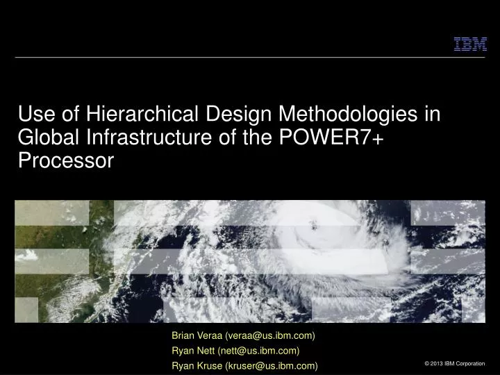
Brian Veraa (veraa@us.ibm.com) Ryan Nett (nett@us.ibm.com) Ryan Kruse (kruser@us.ibm.com). Use of Hierarchical Design Methodologies in Global Infrastructure of the POWER7+ Processor. Introduction. POWER7+ Microprocessor 567mm 2 2.1B devices at 4+GHz core frequency Large global design team

E N D
Brian Veraa (veraa@us.ibm.com) Ryan Nett (nett@us.ibm.com) Ryan Kruse (kruser@us.ibm.com) Use of Hierarchical Design Methodologies in Global Infrastructure of the POWER7+ Processor
Introduction • POWER7+ Microprocessor • 567mm2 • 2.1B devices at 4+GHz core frequency • Large global design team • Hierarchical implementation • Divide and Conquer • Certain global structures span hierarchy • Power • Clock • I/O • We will discuss unique PD challenges presented by these structures • Over/Under booking physical resource • Connectivity across hierarchy • Floorplanning around these structures
POWER7+ Chip Core + Cache Load/Store Unit Core Example of POWER7+ Hierarchy
Clock buffers Power gating circuits Global Infrastructure (G.I.) • Implemented at top level of hierarchy • Clock Distribution • Power Distribution • I/O connections • Load/Store Unit example • First design team delivers LSU • Second design team implements clock distribution at top level • Third design team implements power gating at top level • Many G.I. components fall within physical perimeter of child • Challenge: Communicate physical design data across hierarchy Load/Store Unit (great-grandchild of chip)
Parent Child1 Child2 Communicating PD data across hierarchy: Parent Covers Generate new G.I. abstract • Parent cover represents G.I. content interacting with child • Feedback loop to resolve parent/child conflicts • Used by child for • Floorplanning • Routing • Checking • Multi use children get unioned parent cover Parent Cover Child feeds back change proposals to G.I. owner Parent resolves floorplan conflicts Generate parent cover for child Update child abstract to reflect inverse of parent cover Child respects parent cover during floorplan and routing Parent runs G.I. child collision checking Child runs LVS / DRC
Example of Parent Cover Assembly at Chip Level Load/Store Unit (8 copies) POWER7+ Chip Union 8 copies Load/Store Parent Cover Chip level Power Gate circuits
Challenges with Hierachical Design • Over/Underbooking resource • Connectivity Across Hierarchy • Floorplanning around G.I. Content
Parent Child1 Child2 Overbooking and Underbooking • To enable parallel design work, initial G.I. abstractions are based on estimates • Accuracy of estimates improves over time • Overbooking • Cost is suboptimal utilization • Underbooking • Cost is late design change • Late changes to G.I. abstraction can drive floorplanning, routing, and timing efforts at a schedule sensitive time of the project • The POWER7+ chip team generated parent covers regularly throughout the design cycle to reflect higher quality G.I. component abstracts as their designs matured
Connectivity Across Hierarchy Power connections to G.I. • Certain G.I. components need power connectivity to children • Clock buffers are connected into child power grid • Power gate circuit supplies power to children • Power gate circuit inputs hidden from children Power Path to clock circuits Power Path through power gate circuits Chip Chip C4 via metal Metal (power) metal via via via via via via metal Metal (power) metal via via via via via via Child Unit G.I. Component Child Unit G.I. Component Child Unit metal metal metal metal metal metal via via via via via via metal metal metal metal metal metal via via via via via via metal metal metal metal metal metal via via via via via via metal metal metal metal metal metal Unit Circuits Clock Buffer Unit Circuits Power gate circuit Unit Circuits
Area where both V1 and V2 are present in the parent Short in parent if child connects to it! Parent Inst 1 of child V1 V2 GND Inst 2 of child Unioned shapes (x1,y1) GND exists in only 1 parent instance. Potential DRC or LVS open if child connects to it! (x2,y2) Connectivity Across Hierarchy Checking errors encountered in parent • Case 1: Child contacts V1/V2 pin • Problem: LVS short between V1 and V2 at parent level • Solution: Represent V1/V2 union as blockage, not pins • Case 2: Child contacts GND pin to complete a signal route • Problem 1: LVS open at parent in Inst 2 • Problem 2: DRC error generated at parent in Inst 2 (min area or notch) • Solution: Don’t permit signal routes to contact parent cover
Connectivity Across Hierarchy False checking errors encountered in child Parent Cover V1 (A) V2 V1 V2 • Child contains two power rails: V1, V2 • G.I. content contains only V1 • Pin V1 (A) is connected to V1 grid by layout of G.I. component • Child sees V1 (A) as an LVS open • Checking in parent context is LVS Clean • False opens are communicated to parent to refine parent cover
Floorplanning Around G.I. Content • G.I. circuits consumed a large amount of metal resource • Influenced child floorplanning and route planning. • Congestion analysis • Floorplans were adjusted to minimize the number of flight-lines crossing a particular G.I. component. • In other cases the G.I. was altered. • Consider grouping tightly coupled circuits on the same side of a G.I. component. Load/Store Unit
Conclusion • POWER7+ relied on hierarchical methods to close a large design with a global design team • Concurrent design and schedule closure • Flat design of selected components to meet high performance needs • Management of Global Infrastructure components required: • Effective abstraction • Connectivity modeling across hierarchy • Careful floorplanning • Newer generations of processors are likely to demand more global power and clock management features • More thorough G.I. planning and execution • Better hierarchical interaction management • Techniques and Tools developed by POWER7+ will continue to be leveraged in the future