Download
1 / 74
750 likes | 1k Views
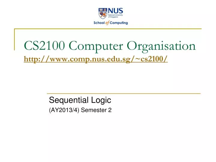
CS2100 Computer Organisation http://www.comp.nus.edu.sg/~cs2100/. Sequential Logic ( AY2013/4) Semester 2. Preparation: 2 weeks. Logic Design: 3 weeks. Computer organisation. WHERE ARE WE NOW?. Number systems and codes Boolean algebra Logic gates and circuits Simplification

E N D
CS2100 Computer Organisationhttp://www.comp.nus.edu.sg/~cs2100/ Sequential Logic (AY2013/4) Semester 2
Preparation: 2 weeks Logic Design: 3 weeks Computer organisation WHERE ARE WE NOW? • Number systems and codes • Boolean algebra • Logic gates and circuits • Simplification • Combinational circuits • Sequential circuits • Performance • Assembly language • The processor: Datapath and control • Pipelining • Memory hierarchy: Cache • Input/output Sequential Logic
SEQUENTIAL LOGIC • Memory Elements • Latches: S-R Latch, D Latch • Flip-flops: S-R flip-flop, D flip-flop, J-K flip-flops, T flip-flops • Asynchronous Inputs • Synchronous Sequential Circuit: Analysis and Design • Memory • Memory Unit • Read/Write Operations • Memory Arrays Sequential Logic
Combinational Logic Combinational Logic inputs inputs : : : : : : : : outputs outputs Memory INTRODUCTION (1/2) • Two classes of logic circuits • Combinational • Sequential • Combinational Circuit • Each output depends entirely on the immediate (present) inputs. • Sequential Circuit • Each output depends on both present inputs and state. Sequential Logic
INTRODUCTION (2/2) • Two types of sequential circuits: • Synchronous: outputs change only at specific time • Asynchronous: outputs change at any time • Multivibrator: a class of sequential circuits • Bistable (2 stable states) • Monostable or one-shot (1 stable state) • Astable (no stable state) • Bistable logic devices • Latches and flip-flops. • They differ in the methods used for changing their state. Sequential Logic
Q Memory element command stored value Q(t) or Q: current state Q(t+1) or Q+: next state MEMORY ELEMENTS (1/3) • Memory element: a device which can remember value indefinitely, or change value on command from its inputs. • Characteristic table: Sequential Logic
Q Memory element command stored value clock Positive pulses Positive edges Negative edges MEMORY ELEMENTS (2/3) • Memory element with clock. • Clock is usually a square wave. Sequential Logic
Positive pulses Positive edges Negative edges MEMORY ELEMENTS (3/3) • Two types of triggering/activation • Pulse-triggered • Edge-triggered • Pulse-triggered • Latches • ON = 1, OFF = 0 • Edge-triggered • Flip-flops • Positive edge-triggered (ON = from 0 to 1; OFF = other time) • Negative edge-triggered (ON = from 1 to 0; OFF = other time) Sequential Logic
S-R LATCH (1/3) • Two inputs:S and R. • Two complementary outputs: Q and Q'. • When Q = HIGH, we say latch is in SET state. • When Q = LOW, we say latch is in RESET state. • For active-high input S-R latch (also known as NOR gate latch) • R = HIGH and S = LOW Q becomes LOW (RESET state) • S = HIGH and R = LOW Q becomes HIGH (SET state) • Both R and S are LOW No change in output Q • Both R and S are HIGH Outputs Q and Q' are both LOW (invalid!) • Drawback: invalid condition exists and must be avoided. Sequential Logic
R 0 1 0 1 0 0 0 1 0 1 Q S R Q Q' Q' 0 1 0 1 0 S 1 0 0 1 0 S-R LATCH (2/3) • Active-high input S-R latch: • Block diagram: Sequential Logic
S R Q Q' S-R LATCH (3/3) • Characteristic table for active-high input S-R latch: Q(t+1) = ? Sequential Logic
S Q Q' R S Q Q' R ACTIVE-LOW S-R LATCH • (You may skip this slide.) • What we have seen is active-high input S-R latch. • There are active-low inputS-R latches, where NAND gates are used instead. See diagram on the left below. • In this case, • when R=0 and S=1, the latch is reset (i.e. Q becomes 0) • when R=1 and S=0, the latch is set (i.e. Q becomes 1) • when S=R=1, it is a no-change command. • when S=R=0, it is an invalid command. • Sometimes, we use the alternative gate diagram for the NAND gate. See diagram on the right above. (This appears in more complex latches/flip-flops in the later slides.) (Sometimes, the inputs are labelled as S' and R'.) Sequential Logic
S Q S EN R Q Q' EN Q' R GATED S-R LATCH • S-R latch + enable input (EN) and 2 NAND gates a gated S-R latch. • Outputs change (if necessary) only when EN is high. Sequential Logic
D Q D EN Q Q' EN Q' GATED D LATCH (1/2) • Make input R equal to S' gated D latch. • D latch eliminates the undesirable condition of invalid state in the S-R latch. Sequential Logic
GATED D LATCH (2/2) • When EN is high, • D = HIGH latch is SET • D = LOW latch is RESET • Hence when EN is high, Q “follows” the D (data) input. • Characteristic table: When EN=1, Q(t+1) = ? Sequential Logic
Clock signal Positive edges Negative edges FLIP-FLOPS (1/2) • Flip-flops are synchronous bistable devices. • Output changes state at a specified point on a triggering input called the clock. • Change state either at the positive (rising) edge, or at the negative (falling) edge of the clock signal. Sequential Logic
S C R J C K D C Q Q' Q Q' Q Q' Positive edge-triggered flip-flops S C R J C K D C Q Q' Q Q' Q Q' Negative edge-triggered flip-flops FLIP-FLOPS (2/2) • S-R flip-flop, D flip-flop, andJ-K flip-flop. • Note the “>” symbol at the clock input. Sequential Logic
S C R Q Q' X = irrelevant (“don’t care”) = clock transition LOW to HIGH S-R FLIP-FLOP • S-R flip-flop: On the triggering edge of the clock pulse, • R = HIGH and S = LOW Q becomes LOW (RESET state) • S = HIGH and R = LOW Q becomes HIGH (SET state) • Both R and S are LOW No change in output Q • Both R and S are HIGH Invalid! • Characteristic table of positive edge-triggered S-R flip-flop: Sequential Logic
D S C R Q Q' CLK = clock transition LOW to HIGH A positive edge-triggered D flip-flop formed with an S-R flip-flop. D FLIP-FLOP (1/2) • D flip-flop: Single input D (data). On the triggering edge of the clock pulse, • D = HIGH Q becomes HIGH (SET state) • D = LOW Q becomes LOW (RESET state) • Hence, Q “follows” D at the clock edge. • Convert S-R flip-flop into a D flip-flop: add an inverter. Sequential Logic
Q1 = X* D CLK D CLK D CLK Q Q' Q Q' Q Q' X Combinational logic circuit Y Q2 = Y* Z Q3 = Z* Transfer * After occurrence of negative-going transition D FLIP-FLOP (2/2) • Application: Parallel data transfer. • To transfer logic-circuit outputs X, Y, Z to flip-flops Q1, Q2 and Q3 for storage. Sequential Logic
J-K FLIP-FLOP (1/2) • J-K flip-flop: Q and Q' are fed back to the pulse-steering NAND gates. • No invalid state. • Include a toggle state • J = HIGH and K = LOW Q becomes HIGH (SET state) • K = HIGH and J = LOW Q becomes LOW (RESET state) • Both J and K are LOW No change in output Q • Both J and K are HIGH Toggle Sequential Logic
J Q Pulse transition detector CLK Q' K J-K FLIP-FLOP (2/2) • J-K flip-flop circuit: • Characteristic table: Q(t+1) = ? Sequential Logic
T T J C K Q Q' Q Pulse transition detector CLK CLK Q' T FLIP-FLOP • T flip-flop: Single input version of the J-K flip-flop, formed by tying both inputs together. • Characteristic table: Q(t+1) = ? Sequential Logic
ASYNCHRONOUS INPUTS (1/2) • S-R, D and J-K inputs are synchronous inputs, as data on these inputs are transferred to the flip-flop’s output only on the triggered edge of the clock pulse. • Asynchronous inputs affect the state of the flip-flop independent of the clock; example: preset (PRE) and clear (CLR) [or direct set (SD) and direct reset (RD)]. • When PRE=HIGH, Q is immediately set to HIGH. • When CLR=HIGH, Q is immediately cleared to LOW. • Flip-flop in normal operation mode when both PRE and CLR are LOW. Sequential Logic
PRE PRE J C K Q Q' J CLR CLR Q Pulse transition detector CLK Q' K CLK PRE CLR Q J = K = HIGH Preset Toggle Clear ASYNCHRONOUS INPUTS (2/2) • A J-K flip-flop with active-low PRESET and CLEAR asynchronous inputs. Sequential Logic
SYNCHRONOUS SEQUENTIAL CIRCUITS • Building blocks: logic gates and flip-flops. • Flip-flops make up the memory while the gates form one or more combinational sub-circuits. • We have discussed S-R flip-flop, J-K flip-flop, D flip-flop and T flip-flop. Sequential Logic
FLIP-FLOP CHARACTERISTIC TABLES • Each type of flip-flop has its own behaviour, shown by its characteristic table. Sequential Logic
SEQUENTIAL CIRCUITS: ANALYSIS (1/7) • Given a sequential circuit diagram, we can analyze its behaviour by deriving its state table and hence its state diagram. • Requires state equations to be derived for the flip-flop inputs, as well as output functions for the circuit outputs other than the flip-flops (if any). • We use A(t) and A(t+1) (or simply A and A+) to represent the present state and next state, respectively, of a flip-flop represented by A. Sequential Logic
x A Q Q D D A' Q' Q' B B' CP y SEQUENTIAL CIRCUITS: ANALYSIS (2/7) • Example using D flip-flops State equations: A+ = A∙x + B∙x B+ = A'∙x Output function: y = (A + B)∙x' Figure 1 Sequential Logic
SEQUENTIAL CIRCUITS: ANALYSIS (3/7) • From the state equations and output function, we derive the state table, consisting of all possible binary combinations of present states and inputs. • State table • Similar to truth table. • Inputs and present state on the left side. • Outputs and next state on the right side. • m flip-flops and n inputs 2m+n rows. Sequential Logic
State equations: A+ = A∙x + B∙x B+ = A'∙x Output function: y = (A + B)∙x' SEQUENTIAL CIRCUITS: ANALYSIS (4/7) • State table for circuit of Figure 1: Sequential Logic
Full table Compact table SEQUENTIAL CIRCUITS: ANALYSIS (5/7) • Alternative form of state table: Sequential Logic
SEQUENTIAL CIRCUITS: ANALYSIS (6/7) • From the state table, we can draw the state diagram. • State diagram • Each state is denoted by a circle. • Each arrow (between two circles) denotes a transition of the sequential circuit (a row in state table). • A label of the form a/b is attached to each arrow where a (if there is one) denotes the inputs while b (if there is one) denotes the outputs of the circuit in that transition. • Each combination of the flip-flop values represents a state. Hence, m flip-flops up to 2m states. Sequential Logic
0/0 1/0 0/1 10 00 1/0 0/1 0/1 1/0 01 1/0 11 SEQUENTIAL CIRCUITS: ANALYSIS (7/7) • State diagram of the circuit of Figure 1: DONE! Sequential Logic
FLIP-FLOP INPUT FUNCTIONS (1/3) • The outputs of a sequential circuit are functions of the present states of the flip-flops and the inputs. These are described algebraically by the circuit output functions. • In Figure 1: y = (A + B)∙x' • The part of the circuit that generates inputs to the flip-flops are described algebraically by the flip-flop input functions (or flip-flop input equations). • The flip-flop input functions determine the next state generation. • From the flip-flop input functions and the characteristic tables of the flip-flops, we obtain the next states of the flip-flops. Sequential Logic
Q J Q' K FLIP-FLOP INPUT FUNCTIONS (2/3) • Example: circuit with a JK flip-flop. • We use 2 letters to denote each flip-flop input: the first letter denotes the input of the flip-flop (J or K for J-K flip-flop, S or R for S-R flip-flop, D for D flip-flop, T for T flip-flop) and the second letter denotes the name of the flip-flop. B C' x JA = B∙C'∙x + B'∙C∙x' KA = B + y A B' C x' B y CP Sequential Logic
Q Q D D x Q' Q' A A' B B' CP y Figure 1 FLIP-FLOP INPUT FUNCTIONS (3/3) • In Figure 1, we obtain the following state equations by observing that Q+ = DQ for a D flip-flop: A+ = A∙x + B∙x (since DA = A∙x + B∙x) B+ = A'∙x (since DB = A'∙x) Sequential Logic
Q Q J J A x Q' Q' K K B Figure 2 CP ANALYSIS: EXAMPLE #2 (1/3) • Given Figure 2, a sequential circuit with two J-K flip-flops A and B, and one input x. • Obtain the flip-flop input functions from the circuit: JA = B JB = x' KA = B∙x' KB = A'∙x + A∙x' = A x Sequential Logic
ANALYSIS: EXAMPLE #2 (2/3) JA = B JB = x' KA = B∙x' KB = A'∙x + A∙x' = A x • Fill the state table using the above functions, knowing the characteristics of the flip-flops used. Sequential Logic
ANALYSIS: EXAMPLE #2 (3/3) • Draw the state diagram from the state table. Sequential Logic
A B Q Q J J Q' Q' K K CP y x Figure 3 ANALYSIS: EXAMPLE #3 (1/3) • Derive the state table and state diagram of this circuit. • Flip-flop input functions: JA = B JB = KB = (A x)' = A∙x + A'∙x' KA = B' Sequential Logic
ANALYSIS: EXAMPLE #3 (2/3) • Flip-flop input functions: JA = B JB = KB = (A x)' = A∙x + A'∙x' KA = B' • State table: Sequential Logic
ANALYSIS: EXAMPLE #3 (3/3) • State diagram: Sequential Logic
FLIP-FLOP EXCITATION TABLES (1/2) • Analysis: Starting from a circuit diagram, derive the state table or state diagram. • Design: Starting from a set of specifications (in the form of state equations, state table, or state diagram), derive the logic circuit. • Characteristic tablesare used in analysis. • Excitation tablesare used in design. Sequential Logic
JK Flip-flop SR Flip-flop D Flip-flop T Flip-flop FLIP-FLOP EXCITATION TABLES (2/2) • Excitation tables: given the required transition from present state to next state, determine the flip-flop input(s). Sequential Logic
SEQUENTIAL CIRCUITS: DESIGN • Design procedure: • Start with circuit specifications – description of circuit behaviour, usually a state diagram or state table. • Derive the state table. • Perform state reduction if necessary. • Perform state assignment. • Determine number of flip-flops and label them. • Choose the type of flip-flop to be used. • Derive circuit excitation and output tables from the state table. • Derive circuit output functions and flip-flop input functions. • Draw the logic diagram. Sequential Logic
0 00 1 1 1 01 11 0 0 1 10 0 DESIGN: EXAMPLE #1 (1/5) • Given the following state diagram, design the sequential circuit using JK flip-flops. Questions: How many flip-flops are needed? How many input variable are there? Sequential Logic
0 00 1 1 1 11 01 0 0 1 10 0 JK Flip-flop’s excitation table. DESIGN: EXAMPLE #1 (2/5) • Circuit state/excitation table, using JK flip-flops. Sequential Logic
B' A B A' Q' Q' Q Q K K J J CP KA JA KB JB A' Combinational circuit External output(s) (none) A B B' x External input(s) What are to go in here? DESIGN: EXAMPLE #1 (3/5) • Block diagram. Sequential Logic
JA = B∙x' B Bx A 00 01 11 10 B 0 1 1 X X B Bx Bx A A 00 01 11 10 B 1 X X A 00 01 11 10 Bx 0 1 X X X X A 0 1 1 00 01 11 10 x A 1 0 1 X X 1 A X X X X JB = x A X X 1 x x KB = (A x)' KA = B∙x x DESIGN: EXAMPLE #1 (4/5) • From state table, get flip-flop input functions. Sequential Logic