Download
1 / 1
10 likes | 144 Views
Japanese Journal of Applied Physics Vol. 45,No. 36, 2006, pp.L977-L979. Tri-Valued Memory Circuit Using MOS-BJT-NDR Circuits Fabricated by Standard SiGe Process. Kun Shan University. Department of Electronic Engineering. Advisor : Kwang-Jow Gan. Student : Chun-Min Wen. Abstract

E N D
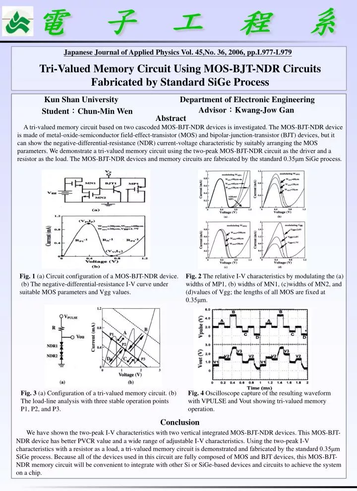
Japanese Journal of Applied Physics Vol. 45,No. 36, 2006, pp.L977-L979 Tri-Valued Memory Circuit Using MOS-BJT-NDR Circuits Fabricated by Standard SiGe Process Kun Shan University Department of Electronic Engineering Advisor:Kwang-Jow Gan Student:Chun-Min Wen Abstract A tri-valued memory circuit based on two cascoded MOS-BJT-NDR devices is investigated. The MOS-BJT-NDR device is made of metal-oxide-semiconductor field-effect-transistor (MOS) and bipolar-junction-transistor (BJT) devices, but it can show the negative-differential-resistance (NDR) current-voltage characteristic by suitably arranging the MOS parameters. We demonstrate a tri-valued memory circuit using the two-peak MOS-BJT-NDR circuit as the driver and a resistor as the load. The MOS-BJT-NDR devices and memory circuits are fabricated by the standard 0.35μm SiGe process. Fig. 1 (a) Circuit configuration of a MOS-BJT-NDR device. (b) The negative-differential-resistance I-V curve under suitable MOS parameters and Vgg values. Fig. 2 The relative I-V characteristics by modulating the (a) widths of MP1, (b) widths of MN1, (c)widths of MN2, and (d)values of Vgg; the lengths of all MOS are fixed at 0.35μm. Fig. 3 (a) Configuration of a tri-valued memory circuit. (b) The load-line analysis with three stable operation points P1, P2, and P3. Fig. 4 Oscilloscope capture of the resulting waveform with VPULSE and Vout showing tri-valued memory operation. Conclusion We have shown the two-peak I-V characteristics with two vertical integrated MOS-BJT-NDR devices. This MOS-BJT-NDR device has better PVCR value and a wide range of adjustable I-V characteristics. Using the two-peak I-V characteristics with a resistor as a load, a tri-valued memory circuit is demonstrated and fabricated by the standard 0.35μm SiGe process. Because all of the devices used in this circuit are fully composed of MOS and BJT devices, this MOS-BJT-NDR memory circuit will be convenient to integrate with other Si or SiGe-based devices and circuits to achieve the system on a chip.