Download
1 / 30
300 likes | 380 Views
Conceptual design of the CLIC DR RF system at 2 GHz. Alexej Grudiev 26 .11.2010 CLIC meeting. Acknowledgements. E. Jensen (CERN) W. Hofle (CERN) K. Akai (KEK). O utline. Introduction H igh stored energy rf system Normal conducting Superconducting Low stored energy rf system

E N D
Conceptual design of the CLIC DR RF system at 2 GHz Alexej Grudiev 26.11.2010 CLIC meeting
Acknowledgements • E. Jensen (CERN) • W. Hofle (CERN) • K. Akai (KEK)
Outline • Introduction • High stored energy rf system • Normal conducting • Superconducting • Low stored energy rf system • Summary
Introduction 1 GHz option, current baseline since March 2010 DR To first order, in steady-state, the energy spread σE/E will be zero BUT the bunch-to-bunch separation can differ from 0.5 ns due to transient beam loading DL To RTML DR 2 GHz option To RTML Specs from RTMLF. Stulle, CLIC meeting, 2010-06-04
CLIC DR RF parameters • *from Yannis on 9/07/2010 • + from Tor et.al., PAC95
CW klystron power supply Information provided by D. Siemaszko LEP klystron power supply Feedback stabilizes high voltage at lower frequencies to the level of 1-0.1%. Limited mainly by the HV measurement accuracy Filter reduce 600 Hz ripples down to 0.04*0.0045 = 2*10-4 filter 12 phases – 600 Hz ripples 3 phases main 4% f t 600 Hz -40 dB t
Klystron amplitude and phase stability Beam voltage ~60 kV Low frequency high voltage stability: 0.1 % (0.3 % achieved in Tristan (KEK) DC power supply for 1MW CW klystron, PAC87) -> 60V -> 1.2 kW rf output power stability ~ 0.3 %power stability ~ 0.15 % amplitude stability Or ~ 1.2 degree phase stability This is not sufficient (see RTML specs). Rf slow feedback loop around the klystron is necessary
Beam cavity interaction, dV/V << 1 Vrf V = Vrf + Vb = V*ejφ dV = dVb*sinφs Vdφ = dVb*cosφs rf phase modulation versus rf amplitude modulation: dφ = dV/(V*tanφs) Energy los per turn: V0 = V sinφs dVb V φs V Vb t dVb dφ
Beam cavity interaction, dV/V << 1 2GHz case 1GHz case W = V2/2ρω; dW = dV 2V/ρω dW/dt = -Pb + ntrains*Tb/Trev*Pb ; dt -> Tb dV/V = -PbTb(1-ntrainsTb/Trev)ρω/V2 dφ = dV/V*1/tanφs Ib Trev Tb t 2GHz case V dφb = dφ+dφs = dV/V*(1/tanφs- tanφs) dV V0 = V sinφs = energy loss per turn = const; dV0 = dVsinφs + Vcosφsdφs = 0 dφs = - dV/V*tanφs Tb Trev t V V0 2GHz case φb φ dφb dφs dφ Tb Trev t
KEKB RF system K. Akai, et. al, “THE LOW-LEVEL RF SYSTEM FOR KEKB”, EPAC98 π/2 - φs dV/V = PbTb(1-Tb/Trev)ρω/V2~ 1 % it is consistent with simulation presented in Fig 3 dφb = dV/V*(1/tanφs – tanφs) ~ 3o it is consistent with simulation presented in Fig 3 Dominated by direct cavity voltage phase modulation in KEKB case
THE ARES CAVITY FOR KEKB, Kageyama et al, APAC98 Scaling of the gap voltage is done to keep heat load per meter constant: P/g = Vg2/2Rgg = Vg2/2ρgQ g => Vg ~1/f3/4 ~2.5 m
CLIC DR parameters for scaled ARES cavity Specs from RTML F. Stulle, CLIC meeting, 2010-06-04 Assuming parameters of ARES cavity from nominal up to tested (150 - 450 kW) and scaled to 1 or 2 GHz dV/V = -PbTb(1-ntrainsTb/Trev)ρgω/VgV dφb = dV/V(1/tanφs-tanφs) Dominated by cavity voltage modulation
Solution 1: Modification of the scaled ARES cavity ρ=V2/2ω(Wa+Ws); in ARES Ws=10Wa If we keep the size of the storage cavity the same as for 0.509 GHz when going to 1 or 2 GHz: Ws=10Wa*(f/0.509)3 ρ=1/f3 In addition, Q-factor improves ~sqrt(f) Scaling of the gap voltage is done to keep heat load per cavity constant: P = Vg2/2Rg= Vg2/2ρgQ => Vg ~1/f5/4 • This implies that we go to higher order mode in storage cavity from TE015 to whispering-gallery modes like in the BOC-type pulse compressor. • Still, shunt impedance drops and wall losses per cavity increase significantly what requires gap voltage reduction.
CLIC DR parameters for modified ARES cavity Specs from RTML F. Stulle, CLIC meeting, 2010-06-04 Assuming parameters of ARES cavity in the range from nominal up to tested and modified to 1 or 2 GHz keeping the same storage cavity volume Performance is almost within specs but the power loss in the cavities is big. It is acceptable for 1 GHz but probably too big for 2 GHz
Solution 2: Mismatchof rf frequency and bunch frequency In the presence of linear phase shift of dφb over a period of time Tb : fb = frf- dφb/2πTb; To compensate dφb= dV/V (1/tanφs- tanφs) = 1.5o at 2 GHz, δV/V = -1%, φs=66o, dfrf/frf = -1.4e-5, very small BUT the associated voltage reduction δV/V results in bucket reduction and consequently in bunch parameters modification. Radiation damping keeps σE=const for all bunches in the train so the bunch length varies along the train. The limit from RTML is that RMS{δσz /σz} < 1% ΔE ΔE/Δz = σE/σz => ΔE σz = Δz σE Variation gives δΔE σz + ΔE δσz = δΔz σE+ Δz δσE Which results in δσz /σz = δΔz/Δz – δΔE/ΔE σE Δz φs=73o Δφ ~ (φs-π/2) δΔφ/Δφ = δφs/(φs-π/2) δφs= -δV/V tanφs δΔφ/Δφ = -δV/V tanφs/(φs-π/2) δV/V = -1%, φs=66o => δΔz/Δz=δΔφ/Δφ = -5.4% σz ΔE2 ~ V(cosφs+(φs-π/2)sinφs) δΔE/ΔE = ½[δV/V+δφs/(tanφs+1/(φs-π/2))] δφs=- δV/V tanφs δΔE/ΔE = ½δV/V[1-1/(1+1/(tanφs(φs-π/2)))] δV/V = -1%, φs=66o => δΔE/ΔE = -8.5% δσz /σz = δΔz/Δz – δΔE/ΔE = -5.4% + 8.5% = 3.1% (peak-to-peak) Image from H. Damerau, PhD Thesis, 2005
Proposal for conceptual design at 2 GHz based on the ARES-type cavities Fix the value of acceptable bunch length increase from first to the last bunch to δσz /σz = 3% This defines allowed voltage reduction δV/V= -1%, which corresponds to dφb= dV/V (1/tanφs- tanφs) = 1.5o, φs = 66o To assure this voltage reduction the total normalized shunt impedance: ρ= -dV/V*V2/(PbTb(1-ntrainsTbfrev) ω) = 25 Ω
RF station layout ARES type cavities beam Reflections from the cavities go to the load Storage cavity Storage cavity Load Circulator Klystron 0.3 MW HVPS 18 kV AC Voltage program input
Superconducting RF option • Making ARES-type cavity superconducting is probably possible but certainly beyond the present state-of-the-art in SC RF technology • Elliptical cavity is an option but it has relatively high normalized shunt impedance. Let’s consider TESLA-like cell: Image and pars from PhysRevSTAB.3.092001 gap
RF station layout for SC cavities beam Reflections from the cavities go to the load Load Circulator Klystron or IOT 60 kW PS 18 kV AC Voltage program input
Scaling of NLC DR RF cavity From PAC 2001, Chicago AN RF CAVITY FOR THE NLC DAMPING RINGS R.A. Rimmer, et al., LBNL, Berkeley, CA 94720, USA From PAC 1995, Collective effects in the NLC DR designs T. Raubenheimer, et al., Scaling of the gap voltage is done to keep heat load per meter constant: P/g = Vg2/2Rgg = Vg2/2ρgQ g => Vg ~1/f3/4
Cavity parameters Number of cavities: N = Vrf/Vg = 4.6/0.23 = 20 = 10 x 2-cells cavities Gap voltage: Vg = Vrf/N = 4.6/20 = 0.23 MV Total wall losses [MW] : P0 = Vrf2/2NR = 4.62/(2*20*1.8) = 0.29 MW Peak beam SR power [MW]: Pb = U0*Ib = 4.2*1.3 = 5.46 MW Matching condition: Total power lost in the cavities when the beam is in: Pin = Pb + P0 = 5.75MW Cavity coupling: β = Q0/Qext = Pin/P0 = (Pb+P0)/P0 = 20 External Q-factor: Qext = Q0/β = 15400/20 = 770 Filling time: tf = Ql/f = Qext/(1+1/β)/f = 770/(1+1/20)/2 GHz = 367 ns Klystron bandwidth: ∂f ∂f >> 1/tf = 1 / 367 = 2.7MHz. AND ∂f >> 1/tgap = 1 / (1402-156) = 0.8 MHz; where tgap – time between the bunch trains RF system total active length: 10 x 1 m = 10 m
Transient beam loading compensation Transient beam loading compensation with infinite bandwidth klystron Amplitude modulation from 1 to 0.55 is necessary (see Vin) Transient beam loading compensation with 0.5% (10 MHz) bandwidth klystron Amplitude modulation from 1 to 0.35 is necessary (see Vin)
Basic layout of 2 GHz rf station 2-cells cavity beam Reflections from the cavities go to the load Circulator Load Klystron 0.6 MW HVPS 80 kV DC Voltage program input 18 kV AC
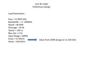
Alternative layout for 2 GHz rf station DR 4-cell cavity beam Reflections from the cavities go to the load Pulse Compressor Load Circulator Alternative layout doubles peak power for a pulse of ~600 ns Klystron 0.6 MW HVPS 80 kV DC 18 kV AC Voltage program input
Klystron bandwidth • NLC DR RF system: • http://www-project.slac.stanford.edu/lc/local/Reviews/cd1%20nov98/RF%20HighPwr_Schwarz.pdf • Klystron • High power CW klystrons of 1 MW output power and -3 MHz 1 dB bandwidth at 700 MHz were developed by industry for APT. • New requirement for Damping Ring klystron is order of magnitude wider bandwidth: 65 nano-seconds gap in between bunch trains cause variations in accelerating field level during bunch train, resulting in bunch extraction phase variation. This effect can be counteracted by a fast direct feedback loop with about 30 MHz bandwidth. • A klystron bandwidth of 20 - 30 MHz is within technical know-how for a 1 MW hiqh power klvstron but will result in lower efficiency. • Klystron Dept. Microwave Engineering, H. Schwarz, 1998 http://ieeexplore.ieee.org/stamp/stamp.jsp?arnumber=01476034 A BROADBAND 500 KW CW KLYSTRON AT S-BAND, Robert H. Giebeler and Jerry Nishida, Varian Associates, Palo Alto, Calif. 1969 klystron amplifier designed for installation ‘on the 210 foot steerable antenna. This paper will describe the development of a 500 kilowatt CW S-band at the JPL/NASA deep space instrumentation facility a€ Goldstone, California. This tube is an improved version of the 450 kilowatt unit developed in 1967. Its features include 1-1/2 percent instantaneous bandwidth, 58 dB nominal gain and 53 percent nominal efficiency. • Few percent bandwidth is feasible for 0.5 MW CW klystron • Most critical issue is to determine peak power versus bandwidth requirements for the low stored energy option.
Summary table All 3 options seems to be feasible but have different issues summarized below φs reduction helps a lot here