Download
1 / 12
120 likes | 123 Views
This design utilizes Xilinx Spartan-3A Evaluation board with on-board Ethernet PHY to implement a MAC stack for TCP/IP communication. It also provides options for RAM and features separate JTAGs for HPTDC. The board uses Spartan-3AN XCS400AN FPGA with non-volatile configuration and supports future options for Spartan6 XC6XLS25T FPGA. The system features unified readout boards with individual Ethernet connections, HPTDC readout control, data reduction, and Ethernet readout protocol implementation. Additionally, an alternative system with a motherboard-daughter card setup is presented.

E N D
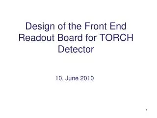
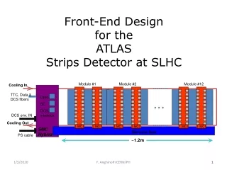
Design of the Front End Readout Board for TORCH Detector 10, June 2010
Based on Xilinx Spartan 3A Evaluation board with on-board 10/100Mbps Ethernet PHY, MAC stack implemented with Xilinx IP core (xps_ethernet_lite) PC using windows data socket for TCP/IP, wincap package for raw MAC packet capture. MAC and Lightweight IP stack with Microblaze processor: 12Mbps MAC stack only with no embedded processor: 60Mbps Conclusion: Raw MAC protocol provides adequate performance but losing the neatness of TCP/IP connection. Ethernet Readout Throughput Test
Board Diagram • MCP connection, • NINO x2, • HPTDCx2 in very high resolution mode, • Medium size Spartan3A/ Small Spartan-6, • Optional RAM, • Separate JTAGs for HPTDC through FPGA, • 40Mhz external clock from motherboard via clock buffer, • Xilinx configuration flash (not needed for Spartan 3AN
Main Components for Front End Readout Board • Spartan 3AN XCS400AN, £21 • 360k block RAM, • 311 user I/O (150 needed), • Non-volatile configuration. • Future choice: Spartan6 XC6XLS25T, Multi-Gigabit transceiver, 930k block RAM. • Gigabit Ethernet Transceiver, £5~20 • National Semiconductor DP83865/ Marvell ME88, Broadcom BCM5461 • Reference design available from Xilinx evaluation boards, • Connectors • Samtec connector for MCP, £3GBP, Lemo 2pin socket £25, • LVDS Clock Buffer, £10 • SN65LVDS104D, • PCB 160mmx 85mm, 8 layers £1000 for 10 boards • Parts cost ~ £200 per boards exclude NINO and HPTDC.
System Features • Unified readout boards to simplify PCB and firmware design, • Each board uses a small – medium size FPGA and has it own Ethernet connection. • PC side need multiple NIC to cope with multiple readout cards from one MCP, • Possibility of using commercial network switch to collect multiple ethernet port in to one is to be investigated.
FPGA Function • HPTDC readout control, • HPTDC JTAG control, • Data FIFO, • Data reduction, • Ethernet readout control and readout protocol implementation,
HPTDC Connection • Two TDC devices, • FPGA as readout controller, • Shared 32-bit parallel data bus, • Individual control bus for each HPTDC.
Roadmap… Schematics Design Layout Design System Evaluation Firmware Design System Testing Board Assembly Software Design
Backup Slides – An alternative system with Motherboard-Daughter Card set up
Readout Daughter Card • Similar to the previous readout card, • No external RAM and no Ethernet interface, • Connect to motherboard via a FIFO interface, • Only need a small FPGA
Motherboard • In addition to the power and clock distribution board, • At lease four Daughter card connections, • Large FPGA, • Fast Ethernet/ Optical link, • Large SDRAM,
System Features • Pros: • Smaller Readout board (Daughter card), • Smaller FPGA, no need of RAM chip • Larger FPGA and SDRAM on mother board allow more buffering and maybe implementation of tcp/ip, • Single cable for one MCP. • Cons: • An extra PCB or integrate the readout motherboard into the PSU/ CLK board, • Extra work in firmware design, • More connections, • Less usable bandwidth – due to the single cable readout.