Download
1 / 8
80 likes | 235 Views
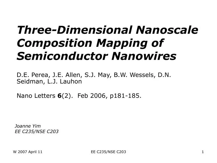
Three-Dimensional Nanoscale Composition Mapping of Semiconductor Nanowires. D.E. Perea, J.E. Allen, S.J. May, B.W. Wessels, D.N. Seidman, L.J. Lauhon Nano Letters 6 (2). Feb 2006, p181-185. Joanne Yim EE C235/NSE C203. Nanowire composition.

E N D
Three-Dimensional Nanoscale Composition Mapping of Semiconductor Nanowires D.E. Perea, J.E. Allen, S.J. May, B.W. Wessels, D.N. Seidman, L.J. Lauhon Nano Letters 6(2). Feb 2006, p181-185. Joanne Yim EE C235/NSE C203 EE C235/NSE C203
Nanowire composition • Compositional flucuations especially critical at nanoscale • Dopants, catalyst, at interface, etc… • Composition mapping tools: • SIMS = secondary ion mass spectroscopy: resolution limited to >100nm • TEM = transmission electron microscopy (Energy Dispersive X-ray Spectroscopy and Electron Energy Loss Spectroscopy): not for volumetric, low concentration. • Averaged over electron beam spot size • Cross sectional Scanning Tunneling Microscopy (XSTM) • Requires making a cross section • 2D EE C235/NSE C203
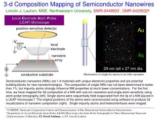
LEAP Microscope • Local Electrode Atom Probe microscope • Sub-nanometer resolution for atom tomography (imaging by sectioning) • Create 3D mapping of composition • First data published from commercial instrument in 2002 3 easy payments of $999,999.95 (prices and participation may vary) EE C235/NSE C203 http://www.imago.com/imago/
microtip sample: ~100nm radius of curvature in UHV chamber • + bias sample, makes positive ions on sample tip • negatively pulsed local electrode tip to induce positive ions to leave • Position sensitive detector collects ions • Lighter mass -> travel faster • Mass-to-charge -> element • Relative composition using counts • Straight line travel -> relative positions EE C235/NSE C203 http://www.imago.com/imago/html/technology/technology.jsp
Experimental • Au seed-catalyzed InAs nanowire growth on GaAs(111)B by MOVPE • Epitaxial, vertical array of nanowires 140um long, spaced 500um apart as defined by initial Au e-beam/liftoff EE C235/NSE C203
SEM (curvature is software artifact) Cross section shows lines corresponding to growth planes (0001) ┴ growth direction spacing of 0.35nm Au atoms (98% In, As removed for picture) EE C235/NSE C203
Catalyst-nanowire interface 23x14x14 nm3 10 nm dia X 1 nm thick slices Interface width <0.5nm www.nsf.gov/mps/dmr/highlights/05highlights/imr/0449933.ppt EE C235/NSE C203
Summary • 3D composition mapping can be achieved • LEAP microscope sample geometry ideal for nanowire morphology • Found Au catalyst incorporated along length of nanowire EE C235/NSE C203