Download
1 / 8
80 likes | 223 Views
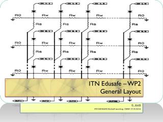
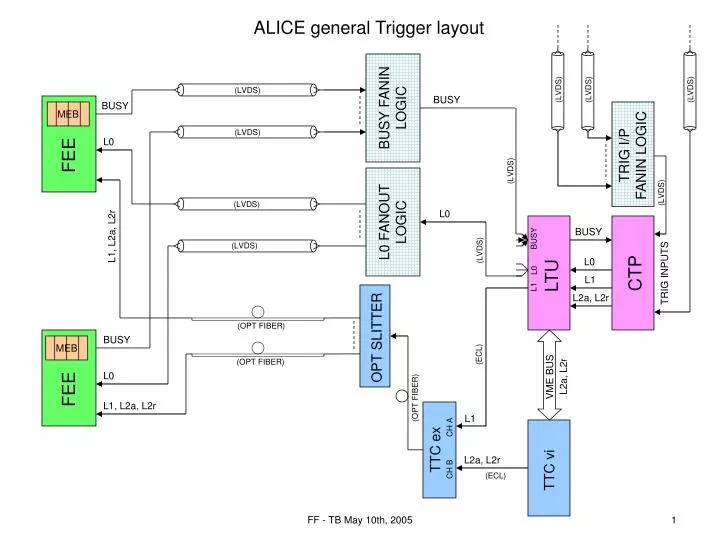
(LVDS). (LVDS). CH A. TTC ex. CH B. MEB. MEB. (LVDS). (LVDS). BUSY FANIN LOGIC. ALICE general Trigger layout. BUSY. BUSY. (LVDS). L0. TRIG I/P FANIN LOGIC. FEE. (LVDS). (LVDS). (LVDS). L0 FANOUT LOGIC. L0. L1, L2a, L2r. BUSY. BUSY. (LVDS). (LVDS). L0. CTP. LTU. L0.

E N D
(LVDS) (LVDS) CH A TTC ex CH B MEB MEB (LVDS) (LVDS) BUSY FANIN LOGIC ALICE general Trigger layout BUSY BUSY (LVDS) L0 TRIG I/P FANIN LOGIC FEE (LVDS) (LVDS) (LVDS) L0 FANOUT LOGIC L0 L1, L2a, L2r BUSY BUSY (LVDS) (LVDS) L0 CTP LTU L0 TRIG INPUTS L1 L1 L2a, L2r (OPT FIBER) OPT SLITTER BUSY (ECL) (OPT FIBER) L2a, L2r L0 VME BUS FEE (OPT FIBER) L1, L2a, L2r L1 L2a, L2r TTC vi (ECL) FF - TB May 10th, 2005
Results of LVDS fan-in/fan-out survey(Orlando’s slide at 11/4/05 TB) FF - TB May 10th, 2005
Conclusions: L0 FANOUT and BUSY + TRIG I/P FANIN units • Proposed technical solution • VME 6U units plugged in LTU partition crates (probably need of 2 more crates) • Fanout: 1 LVDS IN - 12 LVDS OUT (limited by front panel mechanics) • Optional clocked delays to compensate cable lengths (25ns steps, 10-20 steps) • Important: minimum input/output latency required (50ns or better) • Jumpered cable shield GND connection (shorted or through a resistor) • Fanin: 12 LVDS IN - 1 LVDS OUT (limited by front panel mechanics) • Optional remote controlled channel masking • Optional clocked delays to compensate cable lengths (25ns steps, 10-20 steps) • Jumpered cable shield GND connection (shorted or through a resistor) • Compatible signal standard at IN and OUT: same LVDS Tx and Rx as in LTU • same connectors as in LTU • Number of units (from Orlando’s survey) 10 Fanins and 15 Fanouts Detectors asked to agree on technical solution and confirm quantities • Looking for collaborator(s) that are prepared to make the design • Time scale for availability: March 2006 (proto end of 2005) FF - TB May 10th, 2005
LVDS trigger cables Needed for: L0 fanout + Busy fanin + Trigger inputs to CTP Cable lengths of 50 - 70m Compensation at receiver side to correct for: risk of loosing pulses variation of pulse duty cycle Based on passive equalizer to plug in front of the unit receiver connector Measured 100m cable PSpice 100m cable and source models Output of differential Rx (÷10 probe) THR THR End of differential shielded pair FF - TB May 10th, 2005
LVDS transmission • Differential current source transmitter • LVDS Tx Normal typ output current (3.5mA) • LVDM Tx Double typ output current (7mA) • Single 3.3V supply • Differential voltage discriminator receiver • Differential signal hysteresis = 50mV or 100mV • Output high if input unconnected or shorted • Single 3.3V supply Texas Instruments evaluation board Tx = TI 65LVDM31 4 ch, 7mA, LVDS driver tpd = 3ns Max Rx = TI 65LVDS32B 4 ch, 50mV hysteresis, LVDS receiver -2V / +4.4V Common Mode Tpd = 6ns Max Tx Rx Iout Iout Zo tr, tf < 1ns +4.4V 700mV @ Zo=100Ω 50mV 1.2V -2.0V FF - TB May 10th, 2005
Cable equalization principle • Maximization of the media bandwidth according to Max acceptable signal attenuation • Conservation of the cable termination impedance PSpice 100m cable equalization Measured 100m cable attenuation Cable Cable Equalizer -16dB Atten. Equalized cable Equalized cable • -16dB = Max acceptable signal attenuation with: • Worst case (min) current source at Tx (5.4mA for LVDM Tx) • Worst case (max) hysteresis cycle at Rx, times safe margin of 2 (100mV for LVDS Rx) • High impedance cable (120Ω) to maximize signal voltage at Rx (this is also better cable) FF - TB May 10th, 2005
Test results Passive cable equalizer 160pF (150pF) 1.15μH (1μH) 100m Draka Li-2Y(St)H 3x2x0.088mm2 3x shielded twisted pairs Z0 = 120Ω ±10% 262Ω (261Ω) Rx 120Ω 262Ω (261Ω) 148Ω (150Ω) 160pF (150pF) Rx output (÷10 probe) End cable positive signal Without cable equalizer With cable equalizer FF - TB May 10th, 2005
Conclusions: trigger cables • Done simulations and tests of: • 100m Draka Li-2Y(St)H 3x2x0.088mm2 (3x shielded twisted pairs – 4.7ns/m) • Passive cable equalization showed safe working conditions up to 100m: equalizer to be implemented in compact solution • Draka could build single shielded pair with same characteristics for Alice: • under verification through C. Dechelette • Estimated total cable length for whole ALICE: • ~13Km from Orlando’s L0 and Busy table and 50m average per cable • ~2.5Km for the CTP inputs cables (based on 50 Inputs and 50m average) • ~5Km reserve for future use • TOTAL ~ 20Km FF - TB May 10th, 2005