Download
1 / 16
170 likes | 345 Views
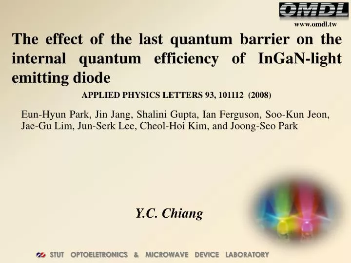
The effect of the last quantum barrier on the internal quantum efficiency of InGaN-light emitting diode. Eun-Hyun Park, Jin Jang, Shalini Gupta, Ian Ferguson, Soo-Kun Jeon, Jae-Gu Lim, Jun-Serk Lee, Cheol-Hoi Kim, and Joong-Seo Park. APPLIED PHYSICS LETTERS 93, 101112 (2008). Y.C. Chiang.

E N D
The effect of the last quantum barrier on the internal quantum efficiency of InGaN-light emitting diode Eun-Hyun Park, Jin Jang, Shalini Gupta, Ian Ferguson, Soo-Kun Jeon, Jae-Gu Lim, Jun-Serk Lee, Cheol-Hoi Kim, and Joong-Seo Park APPLIED PHYSICS LETTERS 93, 101112 (2008) Y.C. Chiang
Outline • Motive • Experimental • Results and Discussion • Conclusions • Extend discussion • Reference
Motive • Improvementin the internal quantum efficiency (IQE) is related low due to: • strong piezoelectric field in MQWs • High dislocation density by heterosubstrate • Unintentional Mg impurity • Mg-doped GaN profile: • deep acceptor • activation process • diffusion
Motive • Improvementin the internal quantum efficiency (IQE) is related low due to: • strong piezoelectric field in MQWs • High dislocation density by heterosubstrate • Unintentional Mg impurity • Mg-doped GaN profile: • deep acceptor • activation process • diffusion
Experimental chip size: 600 x 250 μm2 p-contact Five periods InGaN/GaN(20 Å/100 Å) ITO S1:GaN-LQB (150 Å) S2:In0.03Ga0.97N/GaN LQB(150 Å) p-GaN p~2E19/cm3 In0.27Ga0.73N/GaN n-contact In0.3Ga0.7N/GaN 2μm n-GaN n~3E18/cm3 n-GaN LQB x=0%,1.5%,3%,and 5% 2μm-un-doped GaN 30nm-buffer layer c-plane Sapphire
Results and Discussion(1/5) LQB In含量提高使其較匹配 Mg無法由dislocation竄入井區 V-pit差異不大 由Mg濃度可看出無太大差別 Ref. page 11 FIG. 1. Color online rms roughness(■) and V-shaped pit density(▲) MQWs as indium mole fraction of In(x)Ga(1−x)N-LQB.
Results and Discussion(2/5) (b) 10x10 μm2 AFM surface images of MQWs with GaN-LQB. (c) In0.03Ga0.97N-LQB
① treading dislocations from the buffer layer ② strain relaxation associated with stacking faults on the surface ③ the embedded inclusions within large V-shaped defects that originate at the InGaN-to-GaN interface • A simple schematic diagram to illustrate the growth mechanism: (a) As grown InGaN/GaN, (b) TMIn treatment and inter diffusion
Smooth surface (c) Indium cluster remove, and (d) Indium as surfactant for the grow GaN barrier layer.
Results and Discussion(3/5) Mg~1.2E19/cm3 來自p-GaN diffusion FIG. 2. SIMS profiles of Mg and indium elements of LEDs with GaN-LQB S1 and In0.03Ga0.97N-LQB (S2).
Results and Discussion(4/5) 3.8E18/cm3 5.8E17/cm3 Back FIG. 2. SIMS profiles of Mg and indium elements of LEDs with GaN-LQB S1 and In0.03Ga0.97N-LQB (S2).
Results and Discussion(5/5) S2 High than S1 72% S2 High than S1 15% 不確定是在哪個井區發光,為了要區別所以另外做475nm (b) PL and EL (chip size: 600 x 250 μm2 at 20 mA) (c) spectra of S1(■) and S2(▲) .
Deep-Level 淺層能階 深層能階 淺層能階 Back
Conclusions • A high indium contained LQB made smoother surface of MQWs and shaper interface between MQWs and P-GaN layer by the surfactant role of indium. • A high indium contained LQB could drop the IQE of LED due to the increase in electron overflow to the p-GaN. • Reducing unintentional Mg impurity diffusion into an active layer would be more important.
Extend discussion • 當銦含量逐漸提高,為何使鎂擴散情況降低? • 猜測:因為LQB的銦↑使其和well的不匹配情形稍微降低,也因此dislocationdensity也相對降低,導致鎂比較沒辦法藉由這些缺陷進入到井區。 • 銦含量提高使MQWs表面平整的真正製程原因?(不詳)
References • Eun-Hyun Park, Jin Jang, Shalini Gupta, Ian Ferguson, Soo-Kun Jeon, Jae-Gu Lim, Jun-Serk Lee, Cheol-Hoi Kim, and Joong-Seo Park, “The effect of the last quantum barrier on the internal quantum efficiency of InGaN-light emitting diode,” APPLIED PHYSICS LETTERS 93, 101112 (2008). • 史光國 編譯, “現代半導體發光及雷射二極體材料技術,” 全華科技圖書股份有限公司, 2004.