Download
1 / 37
410 likes | 818 Views
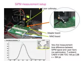
SiPM R&D and MEMS Telescope. Shinwoo Nam Ewha W. University. SiPM MEMS Telescope Our R&D of SiPM for MEMS Telescope. SiPM. Silicon Photomultiplier (G-APD, MPPC). 42 µm. 1 mm. SiPM. 20 µm. 1 mm. 500 ~ 1000 pixels. Pixels of the SiPM. Each pixel : Independent binary device

E N D
SiPM R&D and MEMS Telescope Shinwoo Nam Ewha W. University
SiPM • MEMS Telescope • Our R&D of SiPM for MEMS Telescope
Silicon Photomultiplier (G-APD, MPPC) 42 µm 1 mm SiPM 20 µm 1 mm 500 ~ 1000 pixels Pixels of the SiPM Each pixel : Independent binary device working in Geiger Mode with gain of ~ 10^6 A SiPM output : Sum of all pixels Photon counting
Single Photon Counting Sensors Visible Light Photon Counter Operates at a few Kelvin Hybrid Photodiode Operates with high bias voltage Hamamatsu SiPM
SiPM Micropixel Structure • Breakdown Mode Operation of Micro Cells (PN-junction biased in the reverse direction over the breakdown) • Avalanche region: 0.7~0.8um between p+ and n+ layer with high electric field (3~5)105 V/cm • Drift region: few micron epitaxy layer on low resistive p substrate. • Gain ~106 @ ~50 V working bias • Dark rate(~2 MHz) is originated from thermally produced charge carriers. • Electrical decoupling of the pixels by resistive strips. • Common Al strips for readout. Uniformity of the electric field
Silicon Photomultiplier • Detection efficiency ~25%-60% • Single photon performance (Intrinsic Gain ~106), • Proportional mode for the photon flux (Dynamic range depends on the number of micropixels 500 ~ 3000), • Fast Time response (rising time ~30 ps), • Operation conditions: • Low Operational Voltage ~50-60 V, • Room Temperature, • Non Sensitive to Magnetic Field, • Minimum Required Electronics, • Miniature size and possibility to combine in matrix. • Low cost ( in mass production conditions)
Detection Efficiency • Quantum Efficiency of Micropixel • wavelength and optical absorption function dependent • UV region of Light is limited by present technology topology (dead layer on the top), • IR region of Light is limited by thickness of sensitive layer • Geometry Efficiency • the technology topology gives the limitation of the sensitive area • Breakdown Mode is statistical process • probability that a photoelectron triggers an avalanche process in Si The Depletion Area is ~5 mm: Low Resistive Si, Low Biase Voltage
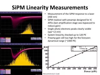
SiPM signal Dark rate signal • Signal of Silicon Photomultiplier with preamplifier (Gain 20) LED Signal LED Signal From V. Saveliev Signal of Silicon Photomultiplier can be readout without Frontend Electronics
Silicon Photomultiplier in Magnetic Field • Silicon Photomultiplier in Strong Magnetic Field Test of SiPM in Strong Magnetic Field up to 4 Tesla (Amplitude of SiPM signal in magnetic field with different orientations) (V. Saveliev, CALICE Meeting, DESY, 30.01.2004)
Silicon Photomultiplier Noise • Dark Count Rate • Probability that bulk thermal electrons trigger an avalanche process (Voltage Dependent) - characterized by frequency • Bias Voltage, Temperature • The noise signal amplitude • is amplitude of single photoelectron • For the measurement of Photons Flux on the level more than ~ 4-5 photoelectrons this dark current factor can be ignored. Hamamatsu
Silicon Photomultiplier Crosstalk • Optic Crosstalk • During avalanche breakdown the micropixel emits photons. These photons should not reach nearby cells because this would initiate breakdowns there. – Optical Crosstalk. Spectrum of Photons emitted during the Avalanche process in Si Hamamatsu ->
Silicon Photomultiplier Applications : HEP • DESY International LInear Collider Group, in particularly Scintillator Tile Hadron Calorimeter Activity Silicon photomultiplier readout of Scintillator Tile with WLS
Silicon Photomultiplier Applications : Medical Instrument • Positron Emission Tomography Spectrums of 22Na (511 keV) with LSO Silicon Photomultiplier is most promising Photodetector for the Modern Scintillator Material and Medical Imaging Systems
Silicon Photomultiplier Applications : Space • SiPM in space Silicon Photomultiplier is most promising Photodetector for the space applicatioin
그림 1). 지구에서 관측된 고에너지 입자의 에너지에 따른 분포 (Nagano & Watson 2000). 그림 1의 y-축에 E3을 곱한 결과이다. Cosmic Ray Flux 4
Extensive Air Shower (EAS) Pierre Auger 1930s • Initiated by Hadronic int. of • Primary with Air Molecules • 1. collimated hadronic core • (charged pions source of • muons) • 2. EM subshowers along the axis • from pi^0 decays • (90% of shower) • ~1010 particles at Ground • from 1019 eV primary CR • Shower Detection • - Fluorescence UV photons • - Particles (muon,e+,e-,photon) • - Cerenkov Radiation
Principle of EUSO :Use whole atmosphere as a detector TPC-like natural chamber 1020 eV
x-t view y-t view Image of Air-shower on Focal Surface simulation Y photoelectrons X time(sec) 50 events of 1020eV proton showers are superimposed on the EUSO focal surface with 192 k pixels. Proton E=1020eV, =60º GTU = 2.5 sec 4
(164PDMs = 0.2M pixels) MAPMT (6x6 pixels) 26.2 mm The Focal Surface : PMT -> SiPM 2.26 m max 5900 PMTs on the focal surface! A pixel side = 0.77 km on ground
Idea of MEMS Tracking Mirror Telescope Air Shower 이동체 광검출기 Photodetector Micromirrors Control Circuit 마이크로미러 VLSI 칩 • Archimedes Mirror : Mirror segments by soldiers • Proposed Mirror : Mirrormirror segments by VLSI • Aberration free focusing, Wide FOV, • Fast Tracking capability
What is MEMS Mirror ? • MEMS (MicroElectroMechanical Systems) • Recent technological advance in silicon industry • Originally developed for optical communication & display industry • Cost effectiveness due to standard silicon fab available • 100x100 mm2 in size or less • Each cell controlled independently • Types • DMD : Digital, electrostatic actuator, TI • Others (Piezoelectric, thermal, membrane, …)
Concept of MEMSTEL (MEMS Space Telescope) MEMS Tracking Mirror Telescope • MEMS compound mirror reflector • Perfect focusing & Tracking capability • Small number of detector/electronics channels ~ 1m x 1m Mirror Array Trigger Detector (poor resolution, wide FOV, PMTs) UHECR (1020 eV) Zoom-in Detector (high resolution, narrow FOV, MAPMTs) fluorescence Cerenkov Earth
Fabricated 2-axis Silicon Analog Micromirror (Ewha) Size of mirror array: 3 mm x 3 mm Tilted comb actuator(mirror plate removed) Torsion spring Mirror plate 8 x 8 mirror mask layout Mirror plate Mirror plate and actuator bonding Addressing line (back side view)
MTEL (Pathfinder) Russian Microsatellite Tatyana-2 (2008.7 발사) 탑재체 : MTEL (MEMS Telescope for Extreme Lightning), 3x3 mm2 aperture 전리층 (ionosphere) 주탑재체 극한 대기현상의 메가번개 Extremely Large Transient Sparks 성층권 (stratosphere) 지상으로 치는 일반 번개 Ewha University, Seoul National University, Moscow State University
Concept of Zoom & Tracking of KAMTEL Trigger Zoom MEMS mirror Array Hole Detector Electronics Trigger Mirror : 1-axis on/off Zoom Mirror : 2-axis analog tilting Detector image
한국우주인임무를 위한 극소형 MEMS 우주망원경 IR camera Spectrophotometer Zoom mirror Trigger mirror Detector Detector (MAPMT) IR camera Trigger mirror Zoom mirror aperture Electronics box(Analog, Digital, MEMS driver)
Design for SiPM - Cross section Contact: Al Conduct: Al Resistor: Poly-Si(1MΩ) SiO2 N+ P+ Epitaxy layer: boron doping Trench: fill Polyimide • Each micropixel is isolated by trench • Resister is formed by Poly silicon. • P+ region of pn junction is a small size than n+ region to reduce leakage current.
Design for SiPM - Mask(7 layers) <N+ implant> <Trench> <P+ implant> <Polyimide> <Resistor> <metal> <Contact>
Design for SiPM- mask Design area 4" wafer 32×32 2×2 4×4 16×16 8×8 ×4
Design for SiPM - Geometrical Efficiency 29 3 23 3 26 32 3 8 4 8 21 Unit : um • Cell area : 32ⅹ35=1120um • Sensitive area : 632um • Metal : 8*8+32*3 = 160 • Resistor : 3*21+5.5*3+26*3-2*6.5 = 144.5 • Trench : 32*3+29*3 = 183 • Total non-sensitive area : 487.5 • Geometrical efficiency(%) = 632.5/1120 *100 = 56.5%
Simulation Study Depletion Depth Electric Field Vertical Profile for SIPM
Simulation of Operation Photon Detection Efficiency IV Characteristics
Our first attempt of SiPM fabrication Wafer condition 1. Si Substrate * Type/Dopant: P(bor) * Thickness: ~550um * Resistivity: 5ohm.cm 2. Epitaxy * Type/Dopant: P(bor) * Thickness: 5um ± 5% * Resistivity: 1~ 5ohm.cm Photo Mask Fabrication 55 Steps SiPM wafer in the final process