Download
1 / 25
280 likes | 643 Views
Chapter 6 Voltage Regulators - Part 2-. Control element for voltage regulator normally has four types of circuitry: • Linear Series • Linear Shunt • Series switching • Shunt switching. Transistor Shunt Regulator. Fig. 6.8 Transistor shunt voltage regulator.

E N D
Chapter 6 Voltage Regulators - Part 2-
Control element for voltage regulator normally has four types of circuitry: • Linear Series • Linear Shunt • Series switching • Shunt switching
Transistor Shunt Regulator Fig. 6.8Transistor shunt voltage regulator. • The control element is a transistor, in parallel with the load. • While, the resistor, RS, is in series with the load. • The operation of the transistor shunt regulator is similar to that of • the transistor series regulator, except that regulation is achieved • by controlling the current through the parallel transistor.
The output voltage to the load is (6-5) This explains that the voltage across the load is set by the Zener diode voltage and the transistor base-emitter voltage. If the load resistance decreases, the load current will be larger at a value of: (6-6)
The increase in load current causes the collector current shunted by the transistor is to be less as expressed in the following formula: (6-9) The current through RS is calculated as follows: (6-10)
Shunt Regulator Fig. 6.9 Block diagram of shunt regulator.
Basic op-amp Shunt Regulator with load resistor Fig. 6.10Transistor shunt voltage regulator. Shunt regulators use a parallel transistor for the control element. If the output voltage changes, the op-amp senses the change and corrects the bias on Q1 to follow. The control element maintains a constant output voltage by varying the collector current in the transistor.
The operation of the circuit is similar to the series regulator, except that regulation is achieved by controlling the current through the parallel transistor Q1 When the output voltage tries to decrease due to a change in input voltage or load current caused by a change in load resistance, the decrease is sensed by R3 and R4.
A feedback voltage obtained from voltage divider R3 and R4 is applied to the op-amp’s non-inverting input and compared to the Zener voltage to control the drive current to the transistor. The difference voltage reduces the op-amp’s output(VB), but increasing the collector voltage. This keeps the load output nearly constant.
(6-11) • With IL andVOUT constant, a change in the input voltage produces a change in shunt current (Is)as follow: • Maximum Load current: (6-12) (6-13)
Switching Regulator A voltage regulator in which the control element operates as a switch. Fig. 6.11 Block representation of three-terminal voltage regulator. • The switching regulator is a type of regulator circuit which • its efficient transfer of power to the load is greater than series • and shunt regulators because the transistor is not always • conducting. • The switching regulator passes voltage to the load in pulses, • which then filtered to provide a smooth dc voltage.
Switching Regulator In a voltage-inverter switching regulator, the output is the opposite polarity of the input. It can be used in conjunction with a positive regulator from the same input source. Inversion occurs because the inductor reverses polarity when the diode conducts, charging the capacitor with the opposite polarity of the input.
All switching regulators control the output voltage by rapidly switching the input voltage on and off with a duty cycle that depends on the load. Because they use high frequency switching, they tend to be electrically noisy. on/off control VOUT
The output voltage is expressed as : • The period in the sum of the on-time and the off-time: • The ratio is called the duty cycle (6-14) (6-15)
A step-down switching regulator controls the output voltage by controlling the duty cycle to a series transistor. The duty cycle changes depending on the load requirement. L reverses polarity Because the transistor is either ON or OFF on all switching regulators, the power dissipated in the transistor is very small and the regulator is very efficient. The pulses are smoothed by an LC filter. off - +
In a step-up switching regulator, the control element operates as a rapidly pulsing switch to ground. The switch on and off times are controlled by the output voltage. L field collapses on C charges Step-up action is due to the fact the inductor changes polarity during switching and adds to VIN. Thus, the output voltage is larger than the input voltage. L field builds C discharges off +- - + on off
IC VOLTAGE REGULATORS • Several types of both linear (series and shunt) and switching regulators are available in integrated circuit (IC) form. • Single IC regulators contain the circuitry for: • reference source, • comparator amplifier, • control device, and; • overload protection. • Generally, the linear regulators are three-terminal devices that provides either positive or negative output voltages that can be either fixed or adjustable.
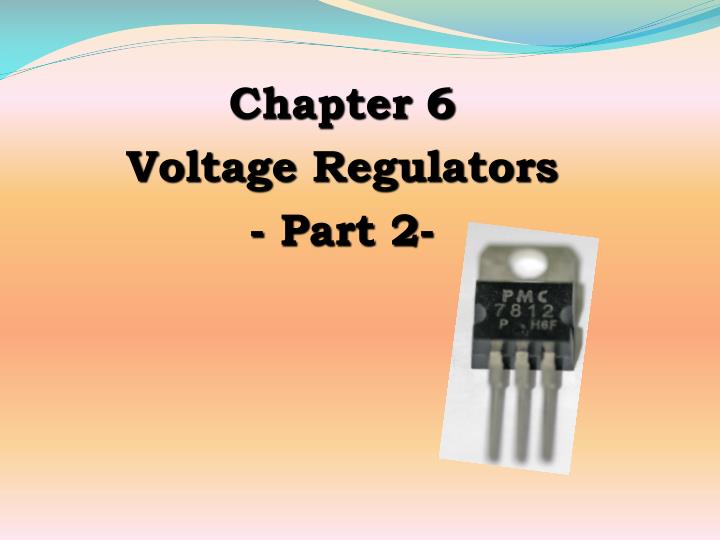
Fixed Voltage Regulator The fixed voltage regulator has an unregulated dc input voltage Vi applied to one input terminal, a regulated output dc voltage Vo from a second terminal, and the third terminal connected to ground. Fixed-Positive Voltage Regulator The series 78XX regulators are the three-terminal devices that provide a fixed positive output voltage. (a) (b) Fig. 6.12 (a) Standard configuration of the series 78XX regulator and (b) typical packages
Fig. 6.12 Standard configuration of a 7812 voltage regulator. The figure above shows: An unregulated input voltage Vi is filtered by a capacitor C1 and connected to the IC’s IN terminal. The IC’s OUT terminal provides a regulated +12 V, which is filtered by capacitor C2. The third IC terminal is connected to ground (GND).
Fixed-Negative Voltage Regulator The series 79XX regulators are the three-terminal IC regulators that provide a fixed negative output voltage. This series has the same features and characteristics as the series 78XX regulators except the pin numbers are different. Fig. 6.14 Standard configuration.
Adjustable-Voltage Regulator Voltage regulators are also available in circuit configurations that allow to set the output voltage to a desired regulated value. The LM317 is an example of an adjustable-voltage regulator, can be operated over the range of voltage from 1.2 to 37 V. Fig. 6.15 Connection of LM317 adjustable-voltage regulator.
The LM317 is a adjustablepositive output IC regulator. There is a fixed reference voltage of +1.25 V between the output andadjustment terminals. There is no ground pin. The output voltage is calculated by: +20 V +16.8 V What is VOUT? (Assume IADJ = 50 mA.) 150 W 150 W 2 kW 2 kW = 16.8 V
End - Chapter 6-