Download
1 / 6
60 likes | 241 Views
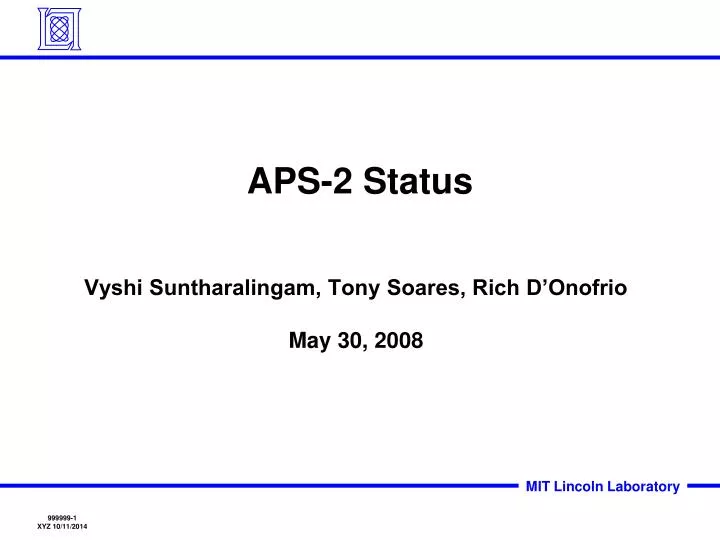
APS-2 Status. Vyshi Suntharalingam, Tony Soares, Rich D’Onofrio May 30, 2008. Status Items. Diode capacitance and leakage extraction Plan for SOI FET noise testing New test board for 3D APS-2 imager chip testing (Tony) We will send a pdf of schematic separately

E N D
APS-2 Status Vyshi Suntharalingam, Tony Soares, Rich D’Onofrio May 30, 2008
Status Items • Diode capacitance and leakage extraction • Plan for SOI FET noise testing • New test board for 3D APS-2 imager chip testing (Tony) • We will send a pdf of schematic separately • Overview of MIT-LL APS-2 testing hardware and software (Rich) • Deliver packaged Back Illuminated imagers (no quartz) • MB21B wafer 9 R5C6 • MB21B wafer 9 R4C3 • MB21A wafer 3 R2C3 • None of these were tested at MIT-LL
Pixel Capacitance and Leakage ExtractionBack Illuminated APS2 Imager Substrate Contact (n+) Ring (VPDBIAS) 4 pixels wide Scupper Pixels (p+) (VSCP) 4 pixels wide 256 x 256 pixel array (p+ side of each diode connected to Tier-2 SOI circuit) C-meter • New measurements with Keithley 4200-SCS (better software and hardware control) • Imager tested after Back Illumination (thinned to 50µm) and pad sputter • Test Area=4160 pixels * (24m)2 • Substrate: n-type 3000 ohm-cm • ~1.5e12 cm-3 • Full depletion not detectable • Dominated by lateral capacitance to Channel Stops • At 10V: 11.5fF/pixel, 70fA/pixel Current(pA/pix)
Insight from Simulation (7/27/07) Doping Profiles Pixel #3 n-CS n-CS (p+) 50 um Depth n-3000 ohm-cm (3e12 /cm3) n-substrate contact 5 x 24 um Width
Two-Dimensional Simulation of 5 PixelsPotential Contours Show Effect of Varying Substrate Bias From 7/27/07 10 “cut-line” Vsub=2V Vsub=5V Vsub=0V 50 (filename error) Vsub=14V 10 10V Potential (V) 5V 2V 0V Vsub=10V Vsub=14V 50 50 Depth into Si Potential profile at center of pixel-3 (vertical “cut-line”) For Vsub=10V, 15V: E-field is vertical from ~25 to 50 um depth into silicon. Nearer to the frontside we observe the lateral influence of the Channel Stops
Reverse Bias of 15V From 7/27/07 15V 0V 0V 0V 15V 8.5 um Microns Clateral Csubstrate 18 Vsub=15V (at backside)