Download
1 / 55
1.28k likes | 2.27k Views
PLD (Programmable Logic Device). ARINDAM CHAKRABORTY LECTURER,DEPT. OF ECE INSTITUTE OF ENGINEERING & MANAGEMENT. IC s Evolution. COMPLEXITY. 1905 : Mount Road -Madras. 2005: Mount Road -Madras. Integrated Circuit Revolution.

E N D
PLD(Programmable Logic Device) ARINDAM CHAKRABORTY LECTURER,DEPT. OF ECE INSTITUTE OF ENGINEERING & MANAGEMENT
COMPLEXITY 1905 : Mount Road -Madras 2005: Mount Road -Madras
Integrated Circuit Revolution 1958:First integrated circuit (germanium) Built by Jack Kilbyat Texas Instruments components :Transistors, Resistors and Capacitors 2000: Intel Pentium 4 Processor Clock speed: 1.5 GHz Transistors: 42 million Technology: 0.18μm CMOS
Evolution of VLSI • SSI–Small Scale Integration (GATE < 10 ) • MSI–Medium Scale Integration (10 < GATE < 1000) • Demanded automation of design process Computer Aid Design started evolving • LSI–Large Scale Integration (GATE > 1000) • VLSI–Very Large Scale Integration ( GATE > 100000)
Before Tools • Laid out 4004 by hand • –Drawn on paper and photographed • –Demagnified 500 times smaller • Almost no verification or validation • –Chips may not function properly • –Market may return products SOLUTION !
Evolution of CAD Tools • VLSI chip design forced • Automation of process • Automation of Simulation based verification • REPLACING • Breadboard Techniques HDL Development
COMPLEXITY 1905 : Mount Road -Madras 2005: Mount Road -Madras
Read Only Memory (ROM) ‘m’ ‘n’ • IT IS TRUTH TABLE IN A HARDWARE FORM • OR • WE CAN SAY HARDWARE FOR TRUTH TABLE ROM A F1 B F2 Ci • SIZE OF ROM:- • FOR, ‘n’ No. OF INPUT AND ‘m’ No. OF OUTPUT • SIZE =2 n x m BITS ROM
Read Only Memory (ROM) DECODER (AND ARRAY) m0 m1 ai Si m2 m3 m4 bi m5 m6 m7 Ci-1 Ci APPLYING 1-BIT FULL ADDER Si = F (1,2,4,7) Ci = F (3,5,6,7) DECODER DESIGN
Read only memory (ROM) • ROM holds programs and data permanently even when computer is switched off • Data can be read by the CPU in any order so ROM is also direct access • The contents of ROM are fixed at the time of manufacture • Access time of between 10 and 50 nanoseconds
PLD (Programmable Logic Device)
PLD • PROGRAMMABLE :: • I CAN CHANGE THE APPLICATION • LOGIC :: • the validity of an argument is determined • by its logical form • DEVICE :: • machine
Programmable Logic Device(PLD): A programmable logic devices is an IC’s that user configurable and is capable of implementing logic function • PLDs ARE :- I . COMBINATIONAL PLDs II . SEQUENTIAL PLDs
I. COMBINATIONAL Programmable Logic Device (PLD):
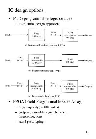
DIFFERENT TYPES OF COMBINATIONAL PLDs :- A. Programmable Read Only Memory (PROM) : Output Input Fixed AND Array (Decoder) Programmable OR Array B. Programmable Array Logic (PAL) : Output Input Programmable AND Array Fixed OR Array C. Programmable Logic Array (PLA) : Output Input Programmable AND Array Programmable OR Array
DIFFERENT TYPEs OF ROM:- ROM (AND & OR ARRAY BOTH ARE FIXED) PROM (FIXED AND ARRAY & PROGRAMMABLE OR ARRAY) EPROM (ERASABLE PROM> TO CHANGE MORE TIME) UVEPROM (OLD TECH.> TO CHANGE THE LOGIC USING UV RAY) EEPROM(ELECTRICALLY ERASABLE PROM> APPLYING ELEC. PULSES) EAPROM(ELECTRICALLY ALTERABLE PROM> NEW TECH) OR FLASH MEMORY
Types of ROM • 1. Programmable Read Only Memory (PROM) • Empty of data when manufactured • May be permanently programmed by the user • 2. Erasable Programmable Read Only Memory (EPROM) • Can be programmed, erased and reprogrammed • The EPROM chip has a small window on top allowing it to be erased by shining ultra-violet light on it • After reprogramming the window is covered to prevent new contents being erased • Access time is around 45 – 90 nanoseconds Note: a nanosecond is one billionth of a second!
Types of ROM • 3. Electrically Erasable Programmable Read Only Memory (EEPROM) • Reprogrammed electrically without using ultraviolet light • Must be removed from the computer and placed in a special machine to do this • Access times between 45 and 200 nanoseconds • 4. Flash ROM • Similar to EEPROM • However, can be reprogrammed while still in the computer • Easier to upgrade programs stored in Flash ROM • Used to store programs in devices • Access time is around 45 – 90 nanoseconds Note: a nanosecond is one billionth of a second!
DIFFERENT TYPES OF COMBINATIONAL PLDs :- A. Programmable Read Only Memory (PROM) : Output Input Fixed AND Array (Decoder) Programmable OR Array
(A) Programmable Read Only Memory (PROM) OR ARRAY AND ARRAY m0 m1 ai m2 m3 m4 bi m5 m6 m7 Ci-1 Si Ci APPLYING 1-BIT FULL ADDER Si = F (1,2,4,7) Ci = F (3,5,6,7) FIXED AND ARRAY & PROGRAMMABLE OR ARRAY
DIFFERENT TYPES OF COMBINATIONAL PLDs :- B. Programmable Array Logic (PAL) : Output Input Programmable AND Array Fixed OR Array
( B) PROGRAMMABLE ARRARY LOGIC ( PAL ) :- X Y Z PAL P0 P1 P2 P3 P4 P5 P1 P0 F1= XY + X’Z F2= Y’ + X’Z F3= XY + Y’Z P3 P2 F1 F2 F3 P5 P4 PROGRAMMABLE AND ARRAY & FIXED OR ARRAY
PAL Table (Specifications): SIZE OF PAL : • 3 INPUTs • 3 OUTPUT • 6 PRODUCT TERM • 2 FOR EACH OUTPUT
DIFFERENT TYPES OF COMBINATIONAL PLDs :- C. Programmable Logic Array (PLA) : Output Input Programmable AND Array Programmable OR Array
( C ) PROGRAMMABLE LOGIC ARRARY ( PLA ) :- OR ARRAY AND ARRAY P0 A P1 B P2 C P3 PRODUCT TERM F1 F2 PROGRAMMABLE AND ARRAY & PROGRAMMABLE OR ARRAY
( C) PROGRAMMABLE LOGIC ARRARY ( PLA ) :- X Y Z PLA P0 P1 P2 P3 F1= XY + X’Z F2= Y’ + X’Z F3= XY + Y’Z P0 P1 F3 F2 P0 F1 P2 P3 P1 PROGRAMMABLE AND ARRAY & PROGRAMMABLE OR ARRAY
PLA Table (Specifications): SIZE OF PLA : • 3 INPUTs • 4 PRODUCT TERM • 3 OUTPUT
Design PAL : PAL Table (Specifications): SIZE OF PAL : • 3 INPUTs • 6 PRODUCT TERM • 3 OUTPUT • 2 FOR EACH OUTPUT F1(a,b,c) = ∑m (0,2) F2(a,b,c) = ∑m (0,3,4) F3(a,b,c) = ∑m (0,3,4,7)
Design PLA : PLA Table (Specifications): SIZE OF PLA : • 3 INPUTs • 6 PRODUCT TERM • 3 OUTPUT F1(a,b,c) = ∑m (0,2) F2(a,b,c) = ∑m (0,3,4) F3(a,b,c) = ∑m (0,3,4,7)
Programmable Array Logic (PAL) & Programmable Logic Array (PLA) :
II . SEQUENTIAL Programmable Logic Device (PLD):
DIFFERENT TYPES OF SEQUENTIAL PLDs :- A. SIMPLE PROGRAMMABLE LOGIC DEVICE (SPLD) : B. COMPLEX PROGRAMMABLE LOGIC DEVICE (CPLD): C. FIELD PROGRAMMABLE GATE ARRAY (FPGA) :
(I) SIMPLE PROGRAMMABLE LOGIC DEVICE (SPLD) :: AND – OR ARRAY (PLA OR PAL) INPUT OUTPUT D- FF • An SPLD can implement hundreds of gates
WHY CPLD? • In case of the 7400 IC, 4 circuits of 2 input NAND gate are housed. In case of 7404, 6 circuits of inverter are housed. • In case of CPLD, it has wiring among the logic in the IC. So, • the wiring on the printed board can be made little.
(II) COMPLEX PROGRAMMABLE LOGIC DEVICE (CPLD):: PLD PLD PLD PLD I/O BLOCK I/O BLOCK PROGRAMMABLE SWITCH MATRIX PLD PLD PLD PLD
Example CPLD Families :: • Altera MAX 7000 and MAX 9000 families • Atmel ATF and ATV families • Lattice ispLSI family • Lattice (Vantis) MACH family • Xilinx XC9500 family
(III) FIELD PROGRAMMABLE GATE ARRAY :: • FPGA, first introduced by Xilinx in 1984. • It is a reprogrammable logic device that implements multilevel logic.
FPGA :: IO IO IO IO IO CLB CLB CLB CLB CLB IO IO CLB CLB CLB CLB CLB IO IO CLB CLB CLB CLB CLB IO IO CLB CLB CLB CLB CLB IO IO • Configurable Logic Block (CLB) • Programmable Interconnect • IO Block IO IO IO IO IO
Elements of an FPGA • Logic Element (LE). • Interconnect. • I/O pins. … … IOB IOB IOB LE LE LE interconnect LE LE LE LE LE LE