Download
1 / 25
250 likes | 426 Views
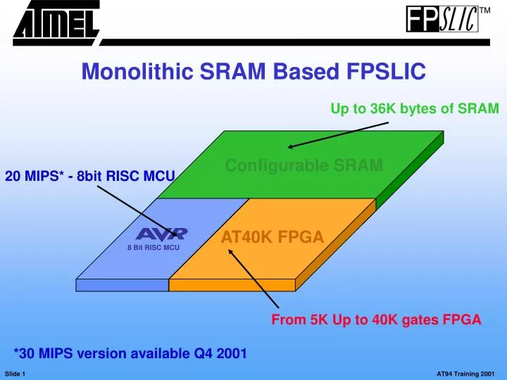
20 MIPS* - 8bit RISC MCU. Up to 36K bytes of SRAM. Configurable SRAM. AT40K FPGA. 8 Bit RISC MCU. From 5K Up to 40K gates FPGA. Monolithic SRAM Based FPSLIC. *30 MIPS version available Q4 2001. Configurable SRAM. SRAM interface. AT40K FPGA. 8 Bit RISC MCU. AVR/AT40K interface.

E N D
20 MIPS* - 8bit RISC MCU Up to 36K bytes of SRAM Configurable SRAM AT40K FPGA 8 Bit RISC MCU From 5K Up to 40K gates FPGA Monolithic SRAM Based FPSLIC *30 MIPS version available Q4 2001
Configurable SRAM SRAM interface AT40K FPGA 8 Bit RISC MCU AVR/AT40K interface FPSLIC Embedded Blocks • Software configurable interface between blocks already implemented • Pre-implemented Interface blocks save 2000-5000 FPGA gates
Designer Allocated Memory 10K* Words Instruction (x 16) PROG. SRAM 2K x 8 2K x 8 2K x 8 Fixed 4K Byte for Data 2K x 8 2Kx 8 2K x 8 Designer Defined Program and Data SRAM Allocation • Memory partition is user defined during development • Easy to trade-off Program and data SRAM * 2K Words (x16) for FPSLIC (AT94K05)
I/O select[15:0] R/W Data[7:0] Int[15:0] AT40K FPGA 8 Bit RISC MCU Internal I/O space and Interrupts Write: ldi r16,0x00 ldi r17,0x02 out FISCR,r16 ; I/O select 0 out FISUA,r17 ; r17 data on the bus 02 Data[7:0] I/Oselect[0] W
Data SRAM (DPRAM) 4K byte up to 16Kbyte Avr-Data[7:0] FPGA-Data[7:0] FPGA-R/W FPGA-Clk FPGA-Add[15:0] AVR-Add[15:0] AVR-R/W AVR-Clk AT40K FPGA 8 Bit RISC MCU Internal Data SRAM Access True Dual Port Access AVR can disable writing from FPGA
AVR System Clk 32 KHz Osc GCLK6 (internal) AVR System Clk AVR System Clk High Frequency Timer Clk 8 Bit RISC MCU WD Clk AVR System Clk AT40K FPGA GCLK5(internal) GCLK 1,2,3,4,7,8 (External) FPSLIC Clocking
FPGA Internal Clocking Scheme • Individual Clock per sector column • Clock and Clock BAR at sector boundary • Column Clock can be any one of 8 Global • clocks • Clock from Column Clock or Express Bus • 4 Fast Clocks (2 per side for PCI spec) • Low power tie-off (lower power!) • Clock skew <1ns guaranteed >> Can reduce power by >50% !
MEM MCU FPGA FPSLIC Reducing Power consumption MCU MEM • Power is reduced • by more than 50% • Standby <100uA • Active 2-3mA/MHz Most of power used in I/O pads ASIC/ FPGA Monolithic Solution Discrete Solution Power is Reduced by 50%+
FPSLIC Reset Pin (External) Configurable SRAM AVR Reset Pin software defined FPGA Logic Reset (any I/O) AT40K FPGA (External) 8 Bit RISC MCU (External) FPSLIC Resets • (Internal) • Watchdog reset AVR only • FPSLIC Software reset with SFTCR bit
Data/Keys Software Application 3 DES RSA Y X[7:0] Y[7:0] Z[7:0] D[7:0] RSA 32 bits 8 Bit RISC MCU write Z X 3 DES FPSLIC - Partial Reconfiguration using AVR CacheLogicTM • Hardware implemented for the AVR to control partial reconfiguration • Enable Hardware context switching
SRAM CONFIGURED AT40K FPGA CONFIGURED 2 Wire FPSLIC- CONFIGURATION ( Mode 0) SRAM SRAM AT40K FPGA AT40K FPGA Configuration Reprogrammed 8 Bit RISC MCU Configurator 2 Wire Protocol • Automatic download after power up --> FPGA bitstream/AVR code and data/System register • EEPROM configuration memory can be updated by FPSLIC itself • Extra system parameters can be stored in remaining EEPROM
5K, 10K and 40K gate AT40K FPGA options High performance AVR microcontroller 2 UARTs, watch-dog timer, programmable timer, interrupt Configuration, 2-wire interface, glue logic Initial AVR-FPSLIC Family
FPSLIC Applications • Wireless and Portable systems • Low power. Stand-by Idd < 100uA. Active <100mA. • Space saving BGA packaging technology • Reconfigurability (on the fly, remote) • Secure FPSLIC for sensitive applications Features: • PDAs and PCMCIA (PCCARD) • Cell phone accessories • Digital cameras • Portable audio • Smartcard readers • Wireless security/access systems • Portable instrumentation • Medical instrumentation • Toll Tags • Irrigation systems/remote monitoring
FPSLIC Applications • Wireline and fixed systems • High performance 20 MIPS @ 25MHz • Remote updates (reconfigurability) • Very flexible architecture - platform product • Space saving BGA packages • Low power. Stand-by Idd < 100uA. Active <100mA • Secure FPSLIC for sensitive applications Features : • Home networking / Internet appliance • Base stations for Wireless systems • Networking and Telecom line-cards • Test equipment • Point of Sale terminals • Wired security/access systems • Industrial control and fixed instrumentation • Image processing systems
Atmel Programmable SLi Roadmap ASIC FPSLICTM /Embeddable FPGA core ASCPs Available now AT40K with ARM ARM FPSLICTM AT40K with RISC uC AVRTM FPSLICTM AT40KxxAX Low $ Features AT40KxxAV Low $ AT40KxxAL Low $ Avail: Now 1.8V 0.12u 1.8V 0.18u 3.3V 0.35u 2000 2001 2002 2003
FPGA AVR Co-Verification FPSLIC™ Design Tools • Complete IDS7 FPGA Software • Place & route, floorplanning, • timing analysis, etc. • Leonardo Spectrum Synthesis Compiler • VHDL & Verilog entry (FPSLIC version) • ModelSim hardware simulator (FPSLIC version) • AVR Studio • Design & debugging • Instruction set simulator • Assembler • Co-verification • PC-based: Windows 95/98/NT/ME/2000 • Powered by Mentor Graphics (FPSLIC version)
FPSLIC™ Software System Designer Modelsim for Simulation $10K value Exemplar’s Leonardo for Synthesis $10K value Co-verification powered by Mentor $50K value AVR Studio for Debug FPGA IDS for Layout
System Designer • Features: • Design Manager • Environment • management • Part Selection Manager • Co-Verification launcher • Launch FPGA/uC tools • Device Dependent • Methodology Manager • Controls System Flow • Bitstream Utilities • Download Utilities • Extensive interactive • help • Intuitive and easy to • learn
Hardware Development Physical Implementation Release to Manufacturing System Integration Software Development Iteration Loop 1 to 3 Months System design without Co-verification
Iteration Loop 1 to 3 Hours Physical Implementation Release to Manufacturing System Integration Co-Verification System design with co-verification System Designer Hardware Development Software Development
Bus Interface Model A P I A P I Model Sim Interface • Peripherals • Bus Cycle Timing • Controllers Co-Verification* Software SW Simulation AVR Studio HDL Simulation ModelSim Co-Verification Software Backplane Instruction-Set Simulator MTI ModelSim Simulator • Complete Instruction Set • Interrupt • Reset • Instruction Timing *FPSLIC Co-Verification S/W is powered by Mentor Graphics
Bitstream Generation Can generate a complete bitstream (AVR and FPGA) or can generate an AVR only or FPGA only bitstream for faster debugging Output file can be directly downloaded to FPSLIC or used on industry standard 3rd part programmers
System Control Register Settings • Everything is programmable in FPSLIC • System Designer gives you control over internal device settings • 64 bits are used for configuring operating Modes • Configuration control • Memory protections and partitioning • Dual pin configuration • I/O drive configuration • Clock selection
System Designer ATDS94KSW1 - $995 Annual Subscription or ATDS94KSW2 - $2495 Purchase Price ATDM94KSW2 - $495 Annual Maintenance Design Tools