Download
1 / 17
170 likes | 247 Views
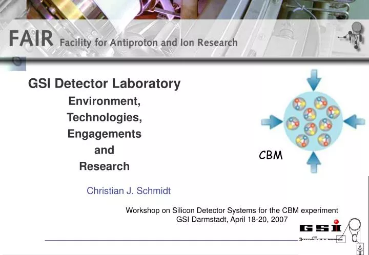
GSI Detector Laboratory Environment, Technologies, Engagements and Research. CBM. Christian J. Schmidt. Workshop on Silicon Detector Systems for the CBM experiment GSI Darmstadt, April 18-20, 2007. Gas Detectors and Wire Chambers at GSI Detector-Lab.

E N D
GSI Detector LaboratoryEnvironment,Technologies, Engagementsand Research CBM Christian J. Schmidt Workshop on Silicon Detector Systems for the CBM experiment GSI Darmstadt, April 18-20, 2007
Gas Detectors and Wire Chambers at GSI Detector-Lab Gas detectors are the traditional stronghold and technological core competence • Various drift chambers for HADES and FOPI at GSI • Large scale production of ALICE TRD chambers ( ~1,5 m2) • R&D and production of ALICE TPC ROC-chambers Wire grid assembly and inspection ALICE TRD comprising 540 TRD modules ALICE TPC ROC
The Start-Veto Device MDCs TOF Spill Monitors, T0, ToF Detectors TOF Shower MDCs START-VETO Beam Veto Start 2 Octogons A 25 x 15 mm dD = 100 µm 1 meter Poly Crystalline CVD Diamond Detectors The world-wide largest CVD-Diamond Detector in Use ! Time-Zero ToF at HADES Poly Crystalline-D Focal Plane Detector for GSI Cave A A = 60 x 40 mm² 32 strips, 1.8 mm pitch dD = 200 µm Cstr= 16.3 pF
Single Crystal- CVD Diamond Detectors for Spectroscopy and Timing exceptional radiation hardness properties
Detectors for Heavy Ion Therapy • Deep engagement and various detector developments at the detector lab for the ion therapy project • Technology transfer to industry • QS and risk-management Beam Monitor PPIC Patient Monitor
12C SIS spill: 108 ions/spill 100 ns/div (top); 5 ns/div (bottom) Diamond Detectors for Tumor Therapy with 12C Ions PC-D Position-Sensitive Carbon-Ion Dosimeters Single-Particle Readout: Precise Fluence Measurements F [ions/cm²] Applied Dose = (DE/ion)*(F/dr)
The GSI Detector-Laboratory Fundamental R&D, Prototyping, Production and Maintenance Traditional expertise and heavy weight upon gas detectors: From beam monitors, wire grids and MWPC to TPC, TRD, RPC and medical applications Fundamental detector R&D and application development for CVD diamond detectors, single crystal and poly-crystalline. Future, FAIR oriented strategic expansion into Silicon strip detector system integration. Large investments planned until 2009 Particular challenge with seamless integration of high density front-end electronics into high rates detector front-end systems People and resources: • 11 staff technicians, engineers and physicists • two PhD students • 12 student workers • 2 to 3 international guests • 1300 m2 laboratory and storage space • Large prototyping CNC mill Operation • Inter collaborative involvement in several experimental endeavors. • Independent funding • Infrastructure responsibilities • Research liberties • Availability of lab space for external groups • Close cooperation with university groups
SIS 100/300 UNILAC SIS 18 CBM ESR HESR PANDA Super FRS RESR CR FLAIR NESR 100 m FAIR - Facility for Antiproton and Ion Research Future facility 2015 GSI today From Anti-Protons to Uranium Project Management: Start of construction: 2007/2008 First beams: 2011 Full operation, CBM: 2015
PANDA Interactions of Anti-Protons with nucleons and nuclei • Universal detector system • Most technologies involved • GSI detector lab engaged in TPC and Silicon Tracker
Development of a TPC for FOPI (GSI) The prototype development for the PANDA TPC DETECTOR-LAB: Challenging project with first large scale employment of n-XYTER FE technology
CBM ECAL (12 m) TOF (10 m) TRDs (4,6, 8 m) RICH dipole magnet beam target STS (5 - 100 cm) Compressed Baryonic Matter Experiment STS zoom-in
7 tracking 6 5 vertexing 4 3 2 1 vacuum pixel detectors z = 5,10,(20) cm micro-strip detectors z = (20),40,60,80,100 cm CBM Silicon Tracking System STS
256 x 256 strips80 µm pitch90 deg stereo angle 256 x 256 strips50 µm pitch90 deg stereo angle 1024 x 1024 strips50 µm pitch15 deg stereo angle 4" wafer, 280 µm thick design finished design finished design partlyfinished Si-Sensor Design: R&D with CIS Erfurt, Germany: (http://www.cismst.de/english/frameset.html) CBM: Opportunity to participate in reseach project of CIS (focus on rad hard detectors). CBM sensor prototypes as "test objects". Sensor design: finished 10/2006.Mid 2007: batch of ~ 20+ wafers. Plenty of sensors for a variety of tests of r/o electronics and detector concept.
n-XYTER: Novel FE-Chip Architecture Cast in Silicon Architectural Solution for CBM and PANDA. Starting point towards the development of the dedicated CBM-XYTER front-end ASIC for several FAIR applications. • detector readout ASIC for high-density and high-rate time and amplitude measurement • 128 channels @ 50 µ pitch • Freely Running, Self Triggered At the GSI Detector Lab: Direct access from chip design into detector prototyping applications. n-XYTER was developed for neutron applications within EU FP-6 NMI3
Near Future • Silicon Prototype production (CIS) • Prototype integration with readout electronics, module prototyping • n – XYTER will serve as prototype for data driven, self triggering readout ASIC • Dedicated ASIC design seeded to result in the CBM-XYTER readout chip. • Prototype beam tests • Supply of local silicon Infrastructure for external collaborators.
Future Detector Laboratory planned upper cleanroom floor ground floor 22m 36 m 700 m2 clean room space (class 10000, locally better) with two main areas reflecting future strategic orientation: solid state detectors and gas detectors Additionally large and high assembly area, mechanics and guest area within clean room space.
Summary • GSI detector laboratory will face many exciting challenges during the research and construction phase of FAIR till 2015 • There will be an essential need for on-site silicon integration facilities as well as know-how. GSI detector lab will respond and strives to be understood also as the local contact for final integration and commissioning of FAIR detector systems. • Silicon system integration will be the strategically novel orientation. • It will be backed with a considerable future investment in infrastructure and clean-room lab space at GSI. • The interwoven marriage of readout electronics and detector devices as with Silicon detectors will break grounds for much closer integration even for gas detectors.