Download
1 / 38
380 likes | 550 Views
The IRS and BLAB3 Deep Storage ASICs for UHE Radio Neutrino and Next Generation Collider Particle Identification. Deeper Sampling CMOS Transient Waveform Recording ASICs. Matt Andrew, Kurtis Nishimura, Gary S. Varner University of Hawai’i, and the

E N D
The IRS and BLAB3 Deep Storage ASICs for UHE Radio Neutrino and Next Generation Collider Particle Identification Deeper Sampling CMOS Transient Waveform Recording ASICs Matt Andrew, Kurtis Nishimura, Gary S. Varner University of Hawai’i, and the Large Area PicosecondPhotoDetector Collaboration TIPP 2011, June 10, 2011
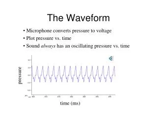
Why Waveform Sampling? • Traditional “crate based” electronics • Gated Analog-to-Digital Converters • Referenced “triggered” Time-to-Digital Converters • High-rate applications • “pipelined operation” • Low-speed, low-resolution sampling • High channel counts • Motivation to reduce cabling • Integrate electronics onto detector elements Q-ADC Det chan TDC Disc. Trigger History FADC Det chan Issues: cost, power, resolution, data volume
Switched Capacitor Array Sampling • Write pointer is ~few switches closed @ once 20fF Input Tiny charge: 1mV ~ 100e- Channel 1 Few 100ps delay Channel 2
“Oscilloscope on a chip” • 2 GSa/s, 1GHz ABW Tektronics Scope • 2.56 GSa/s LAB
An Intrinsic Limitation No power (performance savings) for continuous digitization We aren’t going to put Analog Devices out of business “analog down conversion” For most “triggered” ‘event’ applications, not a serious drawback
Gigasamples/s, but Nyquist? Difficult to couple in Large BW (input C is deadly) • More than 3pF input (ESD protection alone often more) limits ABW < 1GHz • As a result, first generation WFS ASICs a few hundred to 1k samples (ATWD, SAM, DRS, LABRADOR…) • Is this an fundamental limitation? f3dB = 1/2pZC
Why Deeper sampling? ~ km 1018 eVnm
Deeper storage: Buffered LABRADOR (BLAB1) ASIC • Single channel • 64k samples deep, same SCA technique as LAB, no ripple pointer • Multi-MSa/s to Multi-GSa/s • 12-64us to form Global trigger Arranged as 128 x 512 samples Simultaneous Write/Read 3mm x 2.8mm, TSMC 0.25um
BLAB1 High speed Waveform sampling Comparable performance to best CFD + HPTDC MUCH lower power, no need for huge cable plant! Using full samples reduces the impact of noise Photodetector limited CH1 CH2 6.4 psRMS NIM A602 (2009) 438
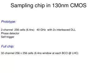
Ice Radio Sampler (IRS) / Buffered LABRADOR 3 (BLAB3) Specifications • Difference between IRS/BLAB • BLAB has input amplifier • IRS doesn’t really use internal trigger capability
Sampling: 128 (2x 64) separate transfer lanes IRS/BLAB3 Single Channel Recording in one set 64, transferring other (“ping-pong” “2 stage sampling”) • Storage: 64 x 512 (512 = 8 * 64) • Wilkinson (32x2): 64 conv/channel
5.82mm 7.62mm IRS/BLAB Die photo 8x RF inputs (die upside down) 32k storage cells per channel (512 groups of 64)
Analog bandwidth Analog BW ~1GHz
Input coupling simulation (35fF sample) Onto chip (flip chip) Magnitude [dB] ~1 GHz stored ARA Trig/Dig Electronics - 17-AUG-2010
Wilkinson ADC – easy to integrate on-chip • No missing codes • Linearity as good as can make ramp • Can bracket range of interest 12-bit ADC • Excellent linearity • Basically as good as can make current source/comparator Run count during ramp Modified! (on-chip clock/counter) [~0.7 GHz]
Storage Cell - compact • Diff. Pair as comparator • Density ~ 25k storage cells/mm^2 (0.25um)
On chipWilkinson Clock ~1us to 9-10 bits ~4us to 12 bits 512 ADC in parallel
Linearity Calibration CAM and/or LUT in FPGA
Example: 100 MHz sine wave input • Need dTcalibrations – but only 128 per channel • Any way to automate? (see K. Nishimura talk)
Not a small effect J. Davies –UC London More like 10% effect at 3.2GSa/s
Now a variety of options… • Success of PSEC3: proof-of-concept of moving toward smaller feature sizes. • Next DRS plans to use 110nm; next SAM plans to use 180 nm.
Expect many other designs in future • Barriers to entry are low • Many different reference designs out there • Challenges (R&D continues): • Fine timing (~ 1ps) • Larger dynamic range • Deeper (continuous) sampling • Faster, sparsifiedreadout • Calibration • Key enabling technology • Large telescope arrays (CTA) • > 100km3 neutrino detectors • PID, Fast x-ray detectors Future Prospects
Top Read Bus Vout=A / (1+A) * Q/Cs =V1 * A/(1+A) Bottom Read BUS 4 Cs Write Bus N capacitors 3 N caps v V1=V Q=Cs.V1 2 1 Return Bus • Track and Hold (T/H) T/H Sampled Data Underlying Technology Analog Input C • Pipelined storage = array of T/H elements, with output buffering
Real MCP-PMT Signals (with BLAB2) Residual Time Walk 7-8 psRMS Rather robust for amplitude invariant signals,TOF still hard, but can shape extract G. Varner -- Deeper Fast Waveform Sampling -- picoSecond WS in Krakow
Simulated Performance vs. SNR 300MHz ABW, 5.9GSa/s G. Varner -- Deeper Fast Waveform Sampling -- picoSecond WS in Krakow
IRS Input Coupling • Input bandwidth depends on 2x terms • f3dB[input] = [2*p*Z*Ctot]-1 • f3dB[storage] = [2*p*Ron*Cstore]-1
Wilkinson Clock Generation • Strictly only 5 channels necessary • 4x antenna, 1x reference channels • Could interleave for twice depth, or multiple reference channels
Wilkinson Recording Ripple counter (run as fast as can) Start = start 0.5-1.5GHz Clock
Triggering • Need 9th channel for monitoring
Triggering – same as previous results • Monitor 9th channel (uses Ch.1 threshold) to compensate for temperature dependence
Assume: 100kHz charged track hits on each bar Hit Processing numbers • ~32 p.e./track (1% of 100ns windows) • 30kHz trigger rate • Each PMT pair sees <8> hits • 240k hits/s • Each BLAB3 has an average occupancy <1 hit (assume 1) • 400ns to convert 256 samples • 16ns/sample to transfer • At least 16 deep buffering • (Markov overflow probability • est. < 10-38) • Each hit = 64samples * 8bits = 512bits • ~125Mbits/s (link is 3.0 Gb/s ~ x30 margin) BLAB3 ASIC Trans-Imp Amps 512 x 64 samples Per channel 8 BLAB3 sampling Fast conversion Matrix (x256) Improvements based upon Lessons learned from BLAB2 Plan to model in standard queuing simulator, but looks like no problem (CF have done same exercise with Jerry Va’vra for 150kHz L1 of SuperB and can handle rate)
Front-end Electronics studies Simulation includes detector response 1GHz analog bandwidth, 5GSa/s J-F Genat, G. Varner, F. Tang, H. Frisch NIM A607 (2009) 387-393. G. Varner and L. Ruckman NIM A602 (2009) 438-445.
Ice Radio Sampler (IRS)RF input coupling (S11) P. Gorham -- measurement
Ice Radio Sampler (IRS) P. Gorham -- measurement
SAM • 1. Maximize dynamic range and minimize signal distorsion. • 2. Minimize need for calibrations and off-chip data corrections. • 3. Minimize costs (both for development & production) • DRS family • Get a solid, general design working • Something that can work, in volume, for many apps • LAB and siblings (68 generations) • Continue to explore parameter space • Concentrate on applications where more general solutions above many not be best choice WFS Evolution and Philosophy Approaches very complementary
PSI activities (DRS) • IEEE/NSS 2008, TIPP09 • http://midas.psi.ch/drs • DAPNIA activities • MATDAQ: IEEE TNS 52-6:2853-2860,2005 / Patent WO022315 • SAM; NIM A567 (2006) 21-26. • Hawaii activities • STRAW: Proc. SPIE 4858-31, 2003. • PRO: JINST, Vol. 3, P12003 (2008). • LABRADOR: NIM A583 (2007) 447-460. • BLAB: NIM A591 (2008) 534-545; NIM A602 (2009) 438-445. • STURM: EPAC08-TUOCM02, June, 2008. References