Download
1 / 13
130 likes | 138 Views
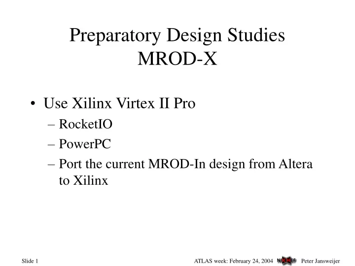
Preparatory Design Studies MROD-X. Use Xilinx Virtex II Pro RocketIO PowerPC Port the current MROD-In design from Altera to Xilinx. Altera APEX20K200EQC240-1 Total logic elements 5605 / 8320 (67 %) Total ESB bits 15360 / 106496 (14 %) Total pins 168 / 171 (98 %). Xilinx

E N D
Preparatory Design StudiesMROD-X • Use Xilinx Virtex II Pro • RocketIO • PowerPC • Port the current MROD-In design from Altera to Xilinx
Altera APEX20K200EQC240-1 Total logic elements 5605 / 8320 (67 %) Total ESB bits 15360 / 106496 (14 %) Total pins 168 / 171 (98 %) Xilinx XC2VP7FG456-7 Number of SLICEs 2898 out of 4928 (58%) Number of RAMB16s 3 out of 44 (6%) Number of External IOBs 168 out of 248 (67%) MROD-In design fromAltera to Xilinx Note 1: Rule of thumb 70 % = FULL. If you try to put more in your FPGA then you’ll probably face routing and timing problems! Note 2: 1 Xilinx “SLICE” (~ 2 “Logic Cells”) ~ 2 Altera “Logic Elements”
GOL to RocketIO test GOL Test Board Development Board Xilinx Virtex-II Pro FPGA Start Insert Error Reset Status LEDs 50 MHz 25 MHz Event Data ROM Altera FPGA Idle 1 Gb/s Run Event Data ROM Rocket IO GOL = ? Okay Fault
GOL to RocketIO testResults • Xilinx ISE RocketIO placement problem -> Solved • Back-annotated simulation (Smart-Models) of the setup -> Okay! Reset Start Insert Error + Start • Real life test -> Okay!
To Be Done:Test FPGA to FPGA Data Links Plus Flow Control Development Board Evaluation Kit Xilinx Virtex-II Pro FPGA Xilinx Virtex-II Pro FPGA 1.6 Gb/s (160 MB/s) Full Empty FIFO Rocket IO Rocket IO FIFO Data Data
PowerPC core Evaluation • Learn to use Xilinx Embedded Development Kit (EDK) • Play with the demos that were delivered with the boards • Made LED On/Off via RS232 system, using PowerPC core + Peripherals.
PPC-Core PLB Arbitter PLB BRAM Controller BRAM PLB 2 OPB Bridge OPB Arbitter Processor Reset UART-Lite JTAG PPC controller Xilinx XC2VP7FF869-6 PPC405s 1 out of 1 100% RAMB16s (2 KByte each) 16 out of 44 36% Number of SLICEs 826 out of 4928 16% PowerPC Hello World System
Conclusions: • Design can easily be ported from Altera to Xilinx • RocketIO • GOL Receiver is working. • Inter FPGA link to be tested. • PowerPC • Consumes FPGA resources (probably need a XC2VP20 instead of a XC2VP7 device) • Needs investment in learning EDK • Needs investment in software development