Download
1 / 24
280 likes | 582 Views
Effects of surface oxide on wafer bonding of GaN and SiC. Jaeseob Lee , Robert F. Davis, and Robert J. Nemanich North Carolina State University Raleigh, NC 27695-8202 USA February 12, 2002. Outline. Motivation - GaN/SiC HBT Introduction - Wafer Bonding of GaN/SiC Experiment

E N D
Effects of surface oxide on wafer bonding of GaN and SiC Jaeseob Lee, Robert F. Davis, and Robert J. Nemanich North Carolina State University Raleigh, NC 27695-8202 USA February 12, 2002
Outline Motivation - GaN/SiC HBT Introduction - Wafer Bonding of GaN/SiC Experiment Results - AES of GaN,SiC - AFM of GaN/SiC - I-V of GaN/SiC Discussion
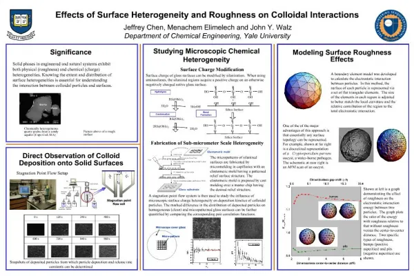
GaN/SiC HBT Advantage of GaN-SiC Device ; high temperature, high power, high frequency operation Larger bandgap emitter -restrict the diffusion of hole from base to emitter → high electron injection efficiency -heavily doped base → low base resistance Indirect bandgap base -longer carrier lifetime(longer diffusion length) → high base transport Short base width higher Emitter efficiency Larger current gain Al Emitter Contact n-GaN Emitter Al/Cr Base Contact p-SiC Base n-SiC Collector Al/Cr Collector Contact GaN/SiC HBT proposed by J. Pankove, S.S. Chang, H.C. Lee, R.J. Moustakas, B. Van Zeghbroeck (Int. Electron Devices Meet Tech. Dig. ’94)
GaN/SiC WB Direct Growth Nucleation Problem Defect due to large mismatch Waferbonding Reduce defect formation at interface No insulating buffer layer between GaN and SiC GaN SiC Buffer Layer(AlN) Growth GaN Buffer Layer acts as a insulator SiC GaN AlN SiC
Ga N Si C Si–N C–Ga C–N Si–Ga Schematic [1120] projection of the GaN/SiC interface GaN/SiC WB
Ex situ Cleaning Characterization (AFM,AES) Ex situ Bonding In situ Annealing Characterization (I-V) Processing Flow Chart Dicing into 12.8×6.5 mm2 pieces Degreasing, HF(SiC)/HCl(GaN) dip N2 blow dry 600, 800, 1000oC, 1hr
AFM of GaN/SiC GaN SiC RMS roughness 20 ± 5 Å in 20×20µm2 area of GaN and SiC
AES of GaN Surface atomic concentration: Cl 0%, C 71%, N 33 8%, O 2 1%, Ga 57 9%
AES of (0001)Si SiC Surface atomic concentration: Si 26 4%, C 20 4%, O 54 4% after HF(100:1) 1min dip Si 21 3%, C 73 13%, O 7 1% after HF( 10:1) 10min dip
Ti n-SiC n-SiC Ti IV of GaN/SiC(n-type to n-type) HF( 10:1) 10min dipped SiC to GaN pair shows more ohmic behavior
Surface Conc. of SiC HF(100:1) dip of (0001)Si/(000-1)C 6HSiC Surface atomic concentration: SiC (0001)Si ; Si 274%, C 15 3%, O 575% after 1min dip Si 214%, C 7614%, O 31% after 60min dip SiC (000-1)C ; Si 234%, C 7313%, O 41% after 1min dip Si 214%, C 7614%, O 31% after 60min dip
6.5 mm 1 mm 12.8 mm WB of GaN/SiC 600oC, 800oC, 1000oC 1hr annealing for WB Ti 1 mm 260 µm nSiC 4~6E18 0.1 µm AlN Conductive 1 µm GaN <1E17 406 µm pSiC 3.5E18 2H GaN(0001)Ga ; Degreasing, HCl 1min dip Pt or Ti p-6H SiC(0001)Si ; Degreasing, HF(10:1) 10min dip
Metal SiC Metal/polished side n-SiC n-SiC p-SiC Ti Ti Pt 800oC 20min IV of metal/SiC 800oC,20min Metal/unpolished side Ohmic contact Ohmic behavior of Metal/SiC
Ti n-SiC n-SiC Ti IV of GaN/SiC(n-type to n-type) (0001)Si, (000-1)C SiC ; HF(10:1) 10min dip (0001)Ga GAN ; HCl 1min dip (0001)C SiC/(0001)Ga GaN pair shows low resistance than(000-1)Si SiC/(0001)Ga GaN pair
Ti Ti n-SiC n-SiC p-SiC p-SiC Ti Pt IV of GaN/SiC(n-type to p-type) 1000ºC 1hr in-situ annealing (0001)C SiC/(0001)Ga GaN pair and (000-1)Si SiC/(0001)Ga GaN pair show rectifying behavior
Ti Ti n-SiC n-SiC p-SiC p-SiC Ti Pt IV of GaN/SiC(n-type to p-type) 800ºC 1hr in-situ annealing (0001)C SiC/(0001)Ga GaN pair shows rectifying behavior But (000-1)Si SiC/(0001)Ga GaN pair shows ohmic behavior
Ti Ti n-SiC n-SiC p-SiC p-SiC Ti Pt IV of GaN/SiC(n-type to p-type) 800ºC 1hr in-situ annealing (0001)C SiC/(0001)Ga GaN pair shows rectifying behavior But (000-1)Si SiC/(0001)Ga GaN pair shows ohmic behavior
5mm 5mm IR image of GaN/SiC 600ºC 1hr in-situ annealing (a) (0001)Si SiC/(0001)GaGaN (b) (000-1)C SiC/(0001)GaGaN (0001)C SiC/(0001)Ga GaN pair and (000-1)Si SiC/(0001)Ga GaN pair do not bond at 600ºC 1hr in-situ annealing
Conclusion Polarity is important factor in WB of SiC/GaN (000-1)C n-SiC/(0001)Ga n-GaN pair has the low resistance (nearly Ohmic) (000-1)C p-SiC/(0001)Ga n-GaN pair keep good rectifying behavior at lower bonding temperature(800oC) No bonding happened at 600oC with wafer surface having RMS roughness 20Å in 20×20µm2.
Future Research Characterize the bonded interface with FiB-TEM Bond patterned GaN structures appropriate for HBT Explore improved polishing of SiC and GaN surface to get low T bonding
1 µm nGaN 4~6E18 0.1µm AlN cunductive Substrate ; 260µm nSiC 4~6E18 Epi 2 ; 0.2 µm pSiC 3.5E18 Epi 1 ; 12.0µm nSiC 6.9E15 Substrate ; 300µm nSiC 4~6E18 Fabrication of HBT 2in From Dr. Davis group From Cree Research Inc.
1 μm nSiC 4~6E18 6.5 mm 0.1 μm AlN Conductive 1 μm nGaN 4~6E18 6.5 mm 0.2 μm pSiC 3.5E18 2 μm 12 μm nSiC 6.9E15 substrate nSiC 4~6E18 300 μm After bonding & Polishing Polishing SiC substrate ; 260µm to 50 µm Bonding Polishing SiC substrate : 50 µm to 2 µm by Diamond lapping film GaN on Si wafer is easy for layer transfer
RIE/metallizing Plan By Parallel-plate RIE RIE RIE Al Al/Cr 0.5 μm nGaN 4~6E18 0.2 μm pSiC 3.5E18 12 μm nSiC 6.9E15 substrate nSiC 4~6E18 Al/Cr Al deposition SF6 500Å/min SiC 20min for 1μm Al/Cr deposition Cl2/Ar 4000Å/min GaN 2.5min for 1μm