Download
1 / 84
921 likes | 1.46k Views
Digital System 數位系統. Chapter 4 Combinational Logic. Ping-Liang Lai ( 賴秉樑 ). Outline of Chapter 4. 4.1 Introduction 4.2 Combination Circuits 4.3 Analysis Procedure 4.4 Design Procedure 4.5 Binary Adder-Subtractor 4.6 Decimal Adder 4.7 Binary Multiplier 4.8 Magnitude Comparator

E N D
Digital System數位系統 Chapter 4 Combinational Logic Ping-Liang Lai (賴秉樑)
Outline of Chapter 4 • 4.1 Introduction • 4.2 Combination Circuits • 4.3 Analysis Procedure • 4.4 Design Procedure • 4.5 Binary Adder-Subtractor • 4.6 Decimal Adder • 4.7 Binary Multiplier • 4.8 Magnitude Comparator • 4.9 Decoders • 4.10 Encoders • 4.11 Multiplexers • 4.12 HDL Models of Combination Circuits
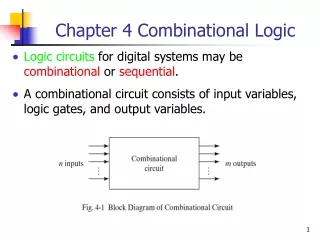
4.1 Introduction (p.138) • Logic circuits for digital systems may be combinational or sequential. • A combinational circuit consists of logic gates whose outputs at any time are determined from only the present combination of inputs.
4.2 Combinational Circuits (p.138) • Logic circuits for digital system • Sequential circuits • Contain memory elements. • The outputs are a function of the current inputs and the state of the memory elements. • The outputs also depend on past inputs.
Combinational Circuits (p.139) • A combinational circuits • 2npossible combinations of input values • Specific functions • Adders, subtractors, comparators, decoders, encoders, and multiplexers. • MSI circuits or standard cells. Combinational Logic Circuit n input variables m output variables ….. ….. Figure 4.1 Block diagram of combinational circuit
4-3 Analysis Procedure (p.139) • A combinational circuit • Make sure that it is combinational not sequential • No feedback path. • Derive its Boolean functions (truth table) • Design verification • A verbal explanation of its function
A Straight-forward Procedure (p.140) • F2 = AB+AC+BC • T1 = A+B+C • T2 = ABC • T3 = F2'T1 • F1 = T3+T2 Figure 4.2 Logic Diagram for Analysis Example
F1 = T3+T2 = F2'T1+ABC = (AB + AC + BC)'(A + B + C) + ABC = (A' + B')(A' + C')(B' + C')(A + B + C) + ABC = (A' + B'C')(AB' + AC' + BC' + B'C) + ABC = A'BC' + A'B'C + AB'C' + ABC • A full-adder • F1: the sum • F2: the carry
The Full-adder • The truth table
4-4 Design Procedure (p.142) • The design procedure of combinational circuits • State the problem (system spec.) • Determine the inputs and outputs • The input and output variables are assigned symbols • Derive the truth table • Derive the simplified Boolean functions • Draw the logic diagram and verify the correctness
Design Procedure • Functional description • Boolean function • HDL (Hardware description language) • Verilog HDL • VHDL • Schematic entry • Logic minimization • Number of gates • Number of inputs to a gate • Propagation delay • Number of interconnection • Limitations of the driving capabilities
Code Conversion Example (p.143) • BCD to excess-3 code • The truth table
The Maps (p.144) Figure 4.3 Maps for BCE to Excess-3 Code Converter
(p.145) • The simplified functions • z = D' • y = CD +C'D' • x = B'C + B'D+BC'D' • w = A+BC+BD • Another implementation • z = D' • y = CD +C'D' = CD + (C+D)' • x = B'C + B'D+BC'D' = B'(C+D) +B(C+D)' • w = A+BC+BD
BCD to Excess-3 • The logic diagram • z = D' • y = CD +C'D' = CD + (C+D)' • x = B'C + B'D+BC'D' = B'(C+D) +B(C+D)‘ • w = A+BC+BD Fig. 4-4 Logic Diagram for BCD to Excess-3 Code Converter
4-5 Binary Adder-Subtractor (p.146) • Half adder • 0 + 0 = 0 ; 0 + 1 = 1 ; 1 + 0 = 1 ; 1 + 1 = 10 • Two input variables: x, y • Two output variables: C (carry), S (sum) • Truth table
Half Adder • S = x'y+xy' • C = xy • The flexibility for implementation • S = xÅy • S = (x+y)(x'+y') • S' = xy+x'y' • S = (C+x'y')' • C = xy = (x'+y')'
Full-Adder (p.147) • Full-Adder • The arithmetic sum of three input bits. • Three input bits • x, y: two significant bits. • z: the carry bit from the previous lower significant bit. • Two output bits: C, S
Full-Adder C S Fig. 4-6 Map for Full Adder Fig. 4-7 Implementation of Full Adder in Sum of Products
Full-Adder • S = x'y'z+x'yz'+ xy'z'+xyz • C = xy+xz+yz • S = zÅ(xÅy) = z'(xy'+x'y)+z(xy'+x'y)'= z'xy'+z'x'y+z((x'+y)(x+y')) = xy'z'+x'yz'+xyz+x'y'z • C = z(xy'+x'y)+xy = xy'z+x'yz+ xy Fig. 4-8 Implementation of Full Adder with Two Half Adders and an OR Gate
Binary Adder (p.149) Figure 4.9 Full-bit adder
Carry propagation • When the correct outputs are available • The critical path counts (the worst case) • (A1, B1, C1) → C2 → C3 → C4 → (C5, S4) • When 4-bits full-adder → 8 gate levels (n-bits: 2n gate levels) Figure 4.10 Full Adder with P and G Shown
Parallel Adders • Reduce the carry propagation delay • Employ faster gates • Look-ahead carry (more complex mechanism, yet faster) • Carry propagate: Pi = AiÅBi • Carry generate: Gi = AiBi • Sum: Si= PiÅCi • Carry: Ci+1 = Gi+PiCi • C0 = Input carry • C1 = G0+P0C0 • C2 = G1+P1C1 = G1+P1(G0+P0C0) = G1+P1G0+P1P0C0 • C3= G2+P2C2 = G2+P2G1+P2P1G0+ P2P1P0C0
Carry Look-ahead Adder (1/2) • Logic diagram Fig. 4.11 Logic Diagram of Carry Look-ahead Generator
Carry Look-ahead Adder (2/2) • 4-bit carry-look ahead adder • Propagation delay of C3, C2 and C1 are equal. Fig. 4.12 4-Bit Adder with Carry Look-ahead
Binary Subtractor • A-B = A+(2’s complement of B) • 4-bit Adder-subtractor • M=0, A+B; M=1, A+(B’+1) Fig. 4.13 4-Bit Adder Subtractor
Overflow • The storage is limited • Add two positive numbers and obtain a negative number • Add two negative numbers and obtain a positive number • V = 0, no overflow; V = 1, overflow • Example:
4-6 Decimal Adder • Add two BCD's • 9 inputs: two BCD's and one carry-in • 5 outputs: one BCD and one carry-out • Design approaches • A truth table with 29 entries • Use binary full Adders • The maximum sum ← 9 + 9 + 1 = 19 • Binary to BCD
BCD Adder (1/3) • BCD Adder: The truth table
BCD Adder (2/3) • Modifications are needed if the sum > 9 • If C = 1, then sum > 9 • K = 1, or • Z8Z4 = 1 (11××), or • Z8Z2 = 1 (1×1×). • Modification: (10)d or + 6 C = K +Z8Z4 + Z8Z2
BCD Adder (3/3) • Block diagram Fig. 4-14 Block Diagram of a BCD Adder
Binary Multiplier (1/2) • Partial products • AND operations Fig. 4.15 Two-bit by two-bit binary multiplier
Binary Multiplier (2/2) • 4-bit by 3-bit binary multiplier Fig. 4.16 Four-bit by three-bit binary multiplier
4-8 Magnitude Comparator • The comparison of two numbers • Outputs: A>B, A=B, A<B • Design Approaches • The truth table of 2n-bit comparator • 22nentries - too cumbersome for large n • Use inherent regularity of the problem • Reduce design efforts • Reduce human errors
Algorithm → logic • A = A3A2A1A0 ; B =B3B2B1B0 • A=B if A3=B3, A2=B2, A1=B1 and A1=B1 • Equality: xi= AiBi+Ai'Bi' • (A=B) = x3x2x1x0=1 • (A>B) = A3B3'+x3A2B2'+x3x2A1B1'+x3x2x1 A0B0' • (A<B) = A3'B3+x3A2'B2+x3x2A1'B1+x3x2x1 A0'B0 • Implementation • xi = (AiBi'+Ai'Bi)'
4-9 Decoder • A n-to-m decoder • A binary code of n bits = 2ndistinct information • N input variables; up to 2noutput lines • Only one output can be active (high) at any time
An implementation Fig. 4.18 Three-to-eight-line decoder
Combinational logic implementation • Each output = a minterm. • Use a decoder and an external OR gate to implement any Boolean function of n input variables.
Demultiplexers • A decoder with an enable input. • Receive information on a single line and transmits it on one of 2npossible output lines. Fig. 4.19 Two-to-four-line decoder with enable input
Decoder/demultiplexers 第三版內容,參考用!
Expansion • Two 3-to-8 decoder: a 4-to-16 decoder Fig. 4.20 4 16 decoder constructed with two 3 8 decoders
Combination Logic Implementation • Each output = a minterm • Use a decoder and an external OR gate to implement any Boolean function of n input variables • A full-adder • S(x, y, z) = S(1,2,4,7) • C(x, y, z) = S(3,5,6,7) Fig. 4.21 Implementation of a full adder with a decoder
Two possible approaches using decoder • OR(minterms of F): k inputs (k minterms) • NOR(minterms of F'): 2nk inputs • In general, it is not a practical implementation
4-10 Encoders • The inverse function of a decoder The encoder can be implemented with three OR gates.
An implementation • Limitations • Illegal input: e.g. D3=D6=1 • The output = 111 (¹3 and ¹6) 第三版內容,參考用!
Priority Encoder • Resolve the ambiguity of illegal inputs • Only one of the input is encoded • D3 has the highest priority • D0 has the lowest priority • X: don't-care conditions • V: valid output indicator
The maps for simplifying outputs x and y Fig. 4.22 Maps for a priority encoder
Implementation of priority Fig. 4.23 Four-input priority encoder