Download
1 / 1
40 likes | 352 Views
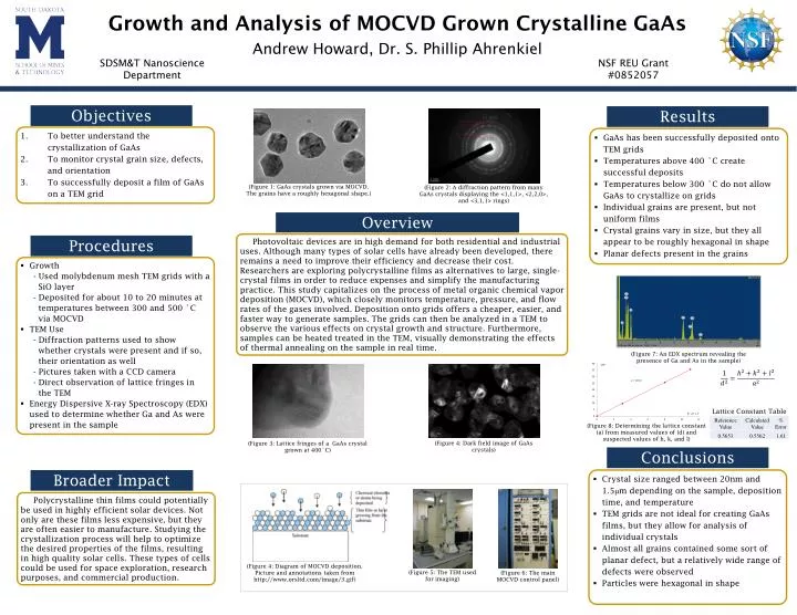
Growth and Analysis of MOCVD Grown C rystalline GaAs. Andrew Howard, Dr. S. Phillip Ahrenkiel. SDSM&T Nanoscience Department. NSF REU Grant #0852057. Objectives. Results. To better understand the crystallization of GaAs To monitor crystal grain size, defects, and orientation

E N D
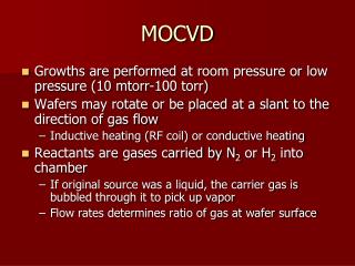
Growth and Analysis of MOCVD Grown Crystalline GaAs Andrew Howard, Dr. S. Phillip Ahrenkiel SDSM&T Nanoscience Department NSF REU Grant #0852057 Objectives Results To better understand the crystallization of GaAs To monitor crystal grain size, defects, and orientation To successfully deposit a film of GaAs on a TEM grid • GaAs has been successfully deposited onto TEM grids • Temperatures above 400 ˚C create successful deposits • Temperatures below 300 ˚C do not allow GaAs to crystallize on grids • Individual grains are present, but not uniform films • Crystal grains vary in size, but they all appear to be roughly hexagonal in shape • Planar defects present in the grains (Figure 1: GaAs crystals grown via MOCVD. The grains have a roughly hexagonal shape.) (Figure 2: A diffraction pattern from many GaAs crystals displaying the <1,1,1>, <2,2,0>, and <3,1,1> rings) Overview Photovoltaic devices are in high demand for both residential and industrial uses. Although many types of solar cells have already been developed, there remains a need to improve their efficiency and decrease their cost. Researchers are exploring polycrystalline films as alternatives to large, single-crystal films in order to reduce expenses and simplify the manufacturing practice. This study capitalizes on the process of metal organic chemical vapor deposition (MOCVD), which closely monitors temperature, pressure, and flow rates of the gases involved. Deposition onto grids offers a cheaper, easier, and faster way to generate samples. The grids can then be analyzed in a TEM to observe the various effects on crystal growth and structure. Furthermore, samples can be heated treated in the TEM, visually demonstrating the effects of thermal annealing on the sample in real time. Procedures • Growth • - Used molybdenum mesh TEM grids with a • SiO layer • - Deposited for about 10 to 20 minutes at • temperatures between 300 and 500 ˚C • via MOCVD • TEM Use • - Diffraction patterns used to show • whether crystals were present and if so, • their orientation as well • - Pictures taken with a CCD camera • - Direct observation of lattice fringes in • the TEM • Energy Dispersive X-ray Spectroscopy (EDX) used to determine whether Ga and As were present in the sample (Figure 7: An EDX spectrum revealing the presence of Ga and As in the sample) Lattice Constant Table (Figure 8: Determining the lattice constant (a) from measured values of (d) and suspected values of h, k, and l) (Figure 4: Dark field image of GaAs crystals) (Figure 3: Lattice fringes of a GaAs crystal grown at 400˚C) Conclusions Broader Impact • Crystal size ranged between 20nm and 1.5μm depending on the sample, deposition time, and temperature • TEM grids are not ideal for creating GaAs films, but they allow for analysis of individual crystals • Almost all grains contained some sort of planar defect, but a relatively wide range of defects were observed • Particles were hexagonal in shape Polycrystalline thin films could potentially be used in highly efficient solar devices. Not only are these films less expensive, but they are often easier to manufacture. Studying the crystallization process will help to optimize the desired properties of the films, resulting in high quality solar cells. These types of cells could be used for space exploration, research purposes, and commercial production. (Figure 4: Diagram of MOCVD deposition. Picture and annotations taken from http://www.orsltd.com/image/3.gif) (Figure 5: The TEM used for imaging) (Figure 6: The main MOCVD control panel)