Download
1 / 11
110 likes | 239 Views
SURFACE TRANSFORMATIONS AND GROWTH OF NANOCRYSTALS ON Au-COVERED GaAs and InP CRYSTALS. Prof. Dr. Imre MOJZES MINAEST-NET TU Berlin/FhG-IZM, Berlin, Germany 22 April 2005. Participants. Imre Mojzes A , Sándor Kökényesi B , István A. Szabó C , Istvan Ivan B , Béla Pécz D

E N D
SURFACE TRANSFORMATIONS AND GROWTH OF NANOCRYSTALSON Au-COVERED GaAs and InP CRYSTALS Prof. Dr. Imre MOJZES MINAEST-NET TU Berlin/FhG-IZM, Berlin, Germany 22 April 2005
Participants • Imre MojzesA, Sándor KökényesiB, István A. SzabóC, Istvan IvanB, Béla PéczD • A – Budapest University of Technology and Economics, • Department of Electronics Technology • H-1111 Budapest Goldmann Gy. ter 3. • mojzes@ett.bme.hu • B –Debrecen University, Department of Experimental Physics • H-4026 Debrecen, Bem ter 18/a Hungary • kiki@tigris.klte.hu • C - Debrecen University, Department of Solid State Physics • H-4010 Debrecen POB 2 Hungary • aszabo@tigris.klte.hu • D – Institute of Technical Physics and Material Sciences • of the Hungarian Academy of Sciences • pecz@mfa.kfki.hu
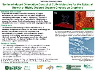
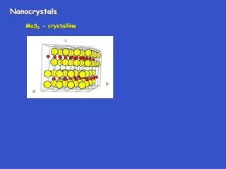
Abstract • We present a simple method of nanocrystal growth during the heating of Au-covered GaAs single crystals in a closed quartz ampoule. The process is the final stage of surface transformations in such crystals which include the disruption of initially continuous, 50 nm thick Au-layer and formation of Au-particle fractals in the relatively low 300-500 oC temperature range and a next step, when a variety of crystalline nanowires and even nanotubes grows on the crystal surface during the further short-period heating up to550-650 oC. These nanostructures were indentified by SEM and TEM measurements as -Ga2O3 and a nonstoichiometric arsenic oxide. It is supposed that the growth of few nanometer thick arsenic oxide tubes follows the vapour-solid mechanism, whereas the catalytic Au-metal growth of thicker -Ga2O3 nanowires was dominated by the vapor-liquid-solid mechanism.
Roots • Interaction of gold based contacts with compound semiconductorsGaAs, InP, InAs, GaSb, InSb, GaP.. • InGaAlAs, GaAsP • GaAs microwave semiconductor devices
Experimental • n – GaAs - 50nm Au • HEATINGquartz ampoule (10-3 torr, H2O, saturated As2)in SEM (high pumping rate) • GaAs, InP
Steps • Sample preparation (Debrecen+Budapest) • Heat teratment (Debrecen) • SEM, HVTEM (Budapest)
Results I. • GaAs/Au nanowires and nanotubs • InP/Au only nanowires
Results II. • GaAs-Au
Results III. • nanotubes
Partners we need • Modelling • Electrical measurements on the nanowires and nanotubes • Application • Fractalmathematical investigations
Contacts • Prof. Dr. Imre MOJZES • Budapest University of Technology and Economics • Department of Electronics TechnologyH-1111 BudapestGoldmann Gy. T. 3. Bld. V2 255.mojzes@ett.bme.hu +36-1-463-2740