Download
1 / 10
100 likes | 222 Views
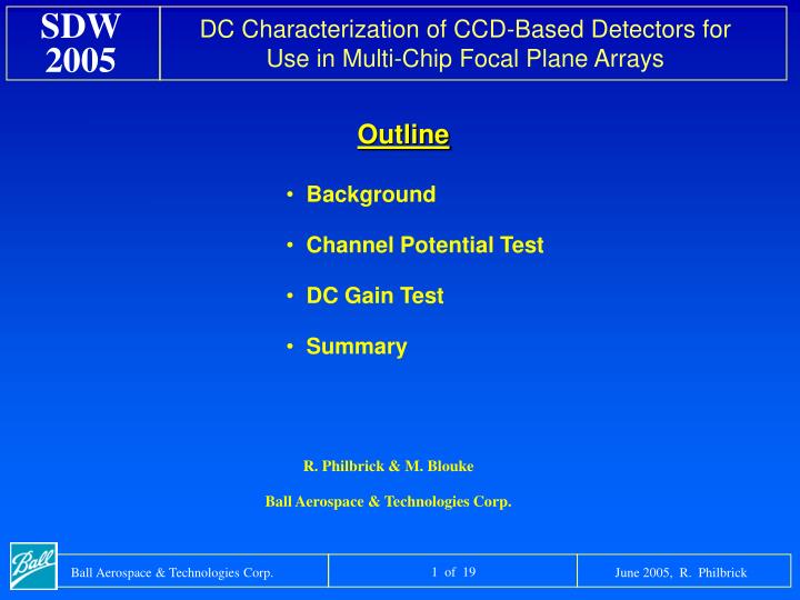
Background Channel Potential Test DC Gain Test Summary. Outline. R. Philbrick & M. Blouke Ball Aerospace & Technologies Corp. Background :.

E N D
Background • Channel Potential Test • DC Gain Test • Summary Outline R. Philbrick & M. Blouke Ball Aerospace & Technologies Corp. Ball Aerospace & Technologies Corp.
Background: • Problem: How to quickly and accurately qualify scientific grade CCDs prior to integration into complex packages and/or multi-chip focal plane arrays (e.g. HiRISE and NPOESS-OMPS )? • Full functional (a.k.a. EO or AC) characterization of incoming CCD detectors can sometimes only be performed after expensive package assembly steps have been completed • Discovering CCD tolerance issues after complex packaging steps is expensive and can significantly impact development schedules • EO testing alone does not adequately reveal all potential problems • For example, if Yth and/or Vin for one clock phase significantly differs from the other clocks or inadequate tolerance range • Performing thorough DC characterization is an effective way to quickly and accurately qualify CCDs HiRISE Multi-Detector FPA NPOESS-OMPS FPA Ball Aerospace & Technologies Corp.
Background: • The DC tests of most interest in detector screening are: • Continuity Yields pin-to-pin resistance, verifies process, checks for gross ESD damage, and verifies detector arrived without damage • Leakage Current Yields static current draw on each gate, checks for subtle ESD damage, and verifies detector arrived without latent damage • Diode Breakdown Verifies process, and confirms adequate operating margins on drain biases (e.g. OD, RD, and ID) • Diode / Opens Checks for open circuits (e.g. bad/missing wirebonds), verifies diode operation, and checks for intra-layer continuity (e.g. poly 1 to poly 1) • Channel Potential Yields threshold potential and inversion voltage for each gate, verifies optimal clock and bias operating points, and confirms tolerance ranges • DC Gain Verifies amplifier operating point and voltage tolerance ranges Ball Aerospace & Technologies Corp.
Channel Potential Test: • Channel Potential (CP) testing yields the threshold potential (Yth) and inversion voltage (Vin) under many, sometimes all, gates on a CCD detector • These two parameters are key for establishing clock and bias operating levels and tolerances • The basic CP measurement requires a gate surrounded by two drains • One drain is statically biased on (“Source” in figure) • A small current is sourced into the other drain (“Drain” in figure), which electrically “floats” to the potential under the controlling gate • Voltage on gate of interest is swept and the “Drain” voltage (i.e. the gate channel potential) is measured • Channel potential testing yields the most information on CCDs with 3 or 4 F architectures, but CCDs with 2 F architectures can also yield significant data • Channel Potential (CP) testing can be performed to some extent on almost all CCD detectors • Most CCD vendors monitor CP test structures on wafers but significant differences from actual CCD data can exist Basic channel potential measurement on a MOSFET Typical channel potential curve Ball Aerospace & Technologies Corp.
Channel Potential Test: • All gates in between the measurement drains, other than the gate being measured, must be turned “on” so they don’t influence results • Other measurement paths must be removed by turning “off” some gates • e.g. If measuring SWA and using two RD drains on either side of the serial register, the parallel register clocks need to be “off” • Typical measurement current is 20 nA • To high a value can induce a significant I.R voltage drop Channel potential setup for Summing Well A (SWA) gate using two amplifier RD drains Ball Aerospace & Technologies Corp.
Channel Potential Test: • Using CP data and design tolerances, complete CP diagrams for the entire CCD can be easily generated • Example here uses +/- 0.1 v design tolerance • Accurately quantifying changes in Yth as a function of radiation exposure level is needed for space-based applications Note the significant shift in serial phase 2 (R2) CP from other serial phases Ball Aerospace & Technologies Corp.
DC Gain Test: • Test measures the small signal gain of each on-chip amplifier by sweeping the reset drain voltage (with reset gate on) and measuring the resultant DC output voltage • Output MOSFET is biased using a constant current load of typically 2 mA • Small signal gain is calculated using • Typical DC gain values range between 0.5 and 0.8 depending on the amplifier configuration (e.g. 1, 2, or 3 stages) • DC gain or equivalent measurements are generally not possible on CMOS based detectors since access to the internal circuitry is limited DC Gain Measurement Setup DC gain test equivalent circuit Ball Aerospace & Technologies Corp.
DC Gain Test: • Any type of CCD charge-to-voltage amplifier can be measured (e.g. single stage, dual stage, and AC coupled stage) • Optimal operating point and adequate bias tolerances can be quickly verified (both pre and post radiation) • “Bad” MOSFETs can be quickly identified Common CCD Output Amplifier Configurations: (a) Single-Stage Source Follower, (b) Two-Stage Source Follower, (c) Two-Stage Source Follower with Bias Control, and (d) AC Coupled, Two-Stage Source Follower Ball Aerospace & Technologies Corp.
DC Gain Test: • A typical input (RD) versus output (OS) curve is shown at right along with small signal gain • Slope of small signal gain curve around operating point gives a measure of the low frequency linearity response Direction of Increasing Signal Output Response and Small Signal Gain for a typical DC coupled amplifier • AC coupled amplifiers yield a slightly different shaped DC gain curve due to the presents of the line reset MOSFET • Two distinct cutoff points are observed • Line reset MOSFET cut off point • Reset MOSFET cut off point • Gate of line reset MOSFET should be held “off” during the entire scan Example of DC gain curve for AC coupled two stage amplifier Ball Aerospace & Technologies Corp.
Summary: • Some examples of problems identified during DC testing • ESD damage occurring during packaging/shipping • Processing problems (e.g. low diode breakdowns) • Non-optimal amplifier operating point • Non-optimal bias levels (e.g. OG, RD or OD) • Inadequate bias tolerances • To account for variability in electronics design, within CCD population, or resulting from post radiation shifts Example of bad recommended DC operating point Non-Optimal OD Operating Point Range Example of bad recommended OD bias point Example of gate to gate channel potential variability Ball Aerospace & Technologies Corp.