Download
1 / 58
640 likes | 898 Views
VLSI Architectures 048878. Lecture 5 Synchronization Background. What is the Problem?. Large chips have multiple clock domains, because: chip interfaces with several unrelated clocks chip integrates IP cores that require different frequencies chip employs dynamic voltage & frequency scaling

E N D
VLSI Architectures048878 Lecture 5 Synchronization Background
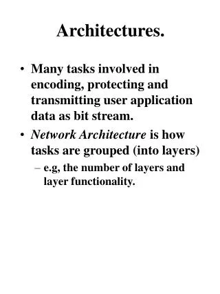
What is the Problem? • Large chips have multiple clock domains, because: • chip interfaces with several unrelated clocks • chip integrates IP cores that require different frequencies • chip employs dynamic voltage & frequency scaling • chip employs local / global clock gating • chip size grows: • Hard to design a LARGE single clock: • Variations (skew, jitter, drift), min / max delays, power, area • More economical to break the chip into multi-sync domains • Cross-domain communications require (clock and/or data) synchronization
Several Unrelated Clocks Example: A Communication Controller / Hub / Bridge 66 MHzPCI 1 MHzCF 12 MbpsUSB 50 MHzMemory 133 MHzCPU 75 MHzDSP 384 Kbps3G 20 MHzFlash Memory 54 Mbps802.11 1 MbpsBluetooth 100 MbpsEtherent a.k.a. MCD: Multiple Clock Domains a.k.a. GALS: Globally Asynchronous, Locally Synchronous
MPSoCheterogeneous P P P P P P P P G CODEC CODEC CODEC P P P P P P P P DSP D DSP P P P P MDM MDM DSP DSP P P P P S M M M M W M M M M M M N XMI XMI DSPCODECMDM Modem M M M M MCS CMP homogeneous P ProcessorM MemoryXMI Ext. Mem. I/FG GraphicsD DisplayS Stream Co-ProcW WirelessN Network
Dynamic Voltage / Frequency Scaling 01000111001110101 50MHz 1.1V 200MHz 1.3V 01000111001110101 100MHz 1.2V 1010 1010 50MHz 1.1V
Clock Large Multi-Sync Chips Thin wires, slow,unbalanceddistributionfor low powerand area Same frequency, different phases MCD / GALS again !
Taxonomy of Multiple Clock Domains clockdomains Single clock domain Multiple clock domains Synchronous Same frequency,different phases Different frequencies Multi-Sync Fixed Frequencies Variable Frequencies Centralcontrol Autonomouscontrol GALS Async domains DVS, DVFS
The Problem: Signal Transfer • Goal: highest BW data • Slow is easy… • If the two clocks are not the same, sampling the data by REG B may fail • We will see how and why REG A REG B data XCLK RCLK
Clock Distribution Networks • Problem Definition • The Technology Roadmap • Standard SoC Clock Trees
IP Coreor Module SoC Global Clock Net Core Internal Clock Net External clock • Core Internal • Clock Driver/PLL: • Buffer • Freq. Multiply • Align PLL Synchronous (single clock domain) SoC
SoC with Multiple Clock Domains Sometimes different domains may physically overlap -- Especially in FPGA
SoC / FPGA Clocking • Full-custom CPU chips employ unique, hand-crafted CDNs (examples below). Too expensive for the rest of us… • SoC CDNs are typically: • generated by CTGen (Cadence), CTS (Synopsys) or similar software • optimized by iterations at the “backend” / “physical design” / “COT” (“customer-owned tools”) stage • ignored at RTL stage (except for methodology) • FPGA clocks are pre-designed • But re-configured with some tools
What’s the Problem ? • Delay variation in clock buffers and lines make it hard to create a perfect synchronous clock • Four types of (clock) delay variations:
Clocks • Clocks should • Provide clocking to the multiple domains • Enable smooth synchronization among domains • Use minimum dynamic power • Use minimum static power • Easiest way to achieve 1+2 is with a single, perfectly-balanced clock • But then you fail on 3+4… • Why? To overcome delay variations, we waste lots of power
Clock Delay Variations • Skew: Static (constant over time) point-to-point variation (of clock arrival time to FFs) • Design variations (unequal wire length, unequal load, IR drop) • Process variations (in-die and die-to-die) • varying L,VT buffer delay variation • varying wire width wire delay variations • Jitter: Cycle-to-cycle variation, limited by design to x% of clock cycle • Data dependent fast changes in VDD, Temp, cross-talk, logic delays • Noise through capacitive and inductive coupling of wires • Drift: Slow change, but can accumulate to large values • Slow changes in VDD, Temp • High Rate: Changes above clock frequency • Switching and harmonics Ginosar & Kol, “Adaptive Synchronization,” ICCD 1998
Design Variation: Weak buffer Design Variation: Unequal load Design Variation: Unequal wire length Design Variation: Unequal # of buffers Design Variation: Balancing wires and buffers Process Variations: L,VT (buffer delay) Process Variations: Wire H,W (wire delay) Clock Delay Variations (1): Static Skew • Stronger buffers overcome these variations • Stronger buffers dissipate more power
Max variations are r% on R, c% on C With variations: Assume std-dev is half max: Actually, even better: More buffers less variation?
More buffers less variation? • Actually, we also add a new source of variation: The buffers themselves • This adds skew, jitter and drift… • But the larger the buffers, the lower the variation • The variance (s2) of L is fixed, not related to the transistor size! Making the transistor wider and longer may reduce the relative effect • This of course adds capacitance increases power… • The effect of VTH variation is not decreased with size, unfortunately
More buffers more power • We still need to drive the entire wire • Dynamic Power = CV2f • And we also need to drive the buffers • About additional 50–100%
How much added power? • The repeaters theory says:
Clock Delay Variations • Skew: Static (constant over time) point-to-point variation (of clock arrival time to FFs) • Design variations (unequal wire length, unequal load, IR drop) • Process variations (in-die and die-to-die) • varying L,VT buffer delay variation • varying wire width wire delay variations • Jitter: Cycle-to-cycle variation, limited by design to x% of clock cycle • Data dependent fast changes in VDD, Temp, cross-talk, logic delays • Noise through capacitive and inductive coupling of wires • Drift: Slow change, but can accumulate to large values • Slow changes in VDD, Temp • High Rate: Changes above clock frequency • Switching and harmonics Ginosar & Kol, “Adaptive Synchronization,” ICCD 1998
Logic Block Data Bus clock branch Clock C/L coupling jitter Data dependent jitter: Power supply coupling Clock Delay Variations (2): Jitter • Stronger buffers and supply overcome jitter • Stronger buffers and supply dissipate more power
Clock Delay Variations • Skew: Static (constant over time) point-to-point variation (of clock arrival time to FFs) • Design variations (unequal wire length, unequal load, IR drop) • Process variations (in-die and die-to-die) • varying L,VT buffer delay variation • varying wire width wire delay variations • Jitter: Cycle-to-cycle variation, limited by design to x% of clock cycle • Data dependent fast changes in VDD, Temp, cross-talk, logic delays • Noise through capacitive and inductive coupling of wires • Drift: Slow change, but can accumulate to large values • Slow changes in VDD, Temp • High Rate: Changes above clock frequency • Switching and harmonics Ginosar & Kol, “Adaptive Synchronization,” ICCD 1998
Drift Vdd Logic Block Clock branch Operation of the logic block results in higher temp, lower Vdd for the clock buffer How fast? Milliseconds, millions of cycles
“PVT” Variations • P—Process • Used to be slow, typical, fast • Now ±kσ (k standard deviations, k2-3) • V—Voltage • Higher voltage faster circuits • T—Temperature • Higher temperature slower circuits • Extremely low temperature and voltage slow circuit
Example: Delay vs. VDD • 90nm, VT=0.2V, VDD=1.0V±20%
Delay Variations Skew Jitter High Rate Drift 1 Log Clock Cycles 0.1 Log R RD Fc R = Rate of Variation Model of Delay Variations • R (rate of variation): • R is NOT the frequency contents of the signal • R is the rate of variation of the propagation delay Ginosar & Kol, “Adaptive Synchronization,” ICCD 1998
Growing Variations Probability 45 66 110 1 / Gate Delay = fT (GHz) C. Visweswariah, IBM, SLIP 2006
High speed,low yield Growing Variations Probability 45 66 110 1 / Gate Delay = fT (GHz) C. Visweswariah, IBM, SLIP 2006
High yield,low speed Growing Variations Probability 45 66 110 1 / Gate Delay = fT (GHz) C. Visweswariah, IBM, SLIP 2006
Relative Clock Skew Clock skew accounts on average for ~5% of the cycle time Sources: ISSCC and JSSC papers; Stefan Rusu, Intel
Why and How Much Variations? • Much, and growing! • Let’s consider the forecast: • ITRS: International Technology Roadmap for Semiconductors (public.itrs.net)
ITRS: The Technology Roadmap • Published every two years (last is 2005, update in 2006) • Industry driven: fabs, equipment, EDA, design, testing, integrated companies (Intel,…) • 15 years outlook (6 short-term, 9 long-term): • 1 year sample to production • 2 years to finalize process • 2 years to build fab, develop process • 2 years to develop equipment • 2 years R&D equipment • 4 years research… • Closely followed by industry: Not an empty prediction, but an actual planning
Rule 1: Scaling (Moore’s Law) • Technology progresses in “cycles” (“nodes”) • Scaling down of feature size by S per cycle
Wire versus gate delays Mark Bohr, Intel; reprinted in ITRS 2001
Path delays can be measures in FO4 delays: Total: 33 x FO4 Supposed to be the same over all technologies The FO4 delay FO4: Delay of a gate driving Fan-Out 4x its size
ITRS: Four product areas • DRAM: Highest density, special niche • Analog / Mixed signal: LNA, PA, VCO, ADC • Challenges: Automated design (lack of designers), low Vdd, high device variation, high noise, high leakage, SOC integration • High speed microprocessors (MPU) • 300 mm2 area, highest density, highest clock rates • SOC (used to be ASIC) • Smaller dies (5-50Mtx/2001), clock 10% of max, low power
What’s ASIC / SoC ? • Two meanings: • A business model • A design methodology
The ASIC Business Model • Break ASIC projects among different horizontal divisions / companies • System: Spec • Logic: RTL design (Verilog / VHDL) and verification • Backend / Physical: Convert RTL to mask data • Fab: Create mask, fabricate wafers, production test • Package • Test / Qual / Product engineering
The ASIC / SoC Methodology • Verilog/VHDL or higher level languages • Automatic logic synthesis • Standard cell libraries, IP Cores • Custom functions rarely created • Goals: Low design cost and risk • Conservative design methods • Lower clock frequency and layout density than MPU • Fast clock cycle time: • 20 FO4 in MPU • 100++ FO4 in SoC • Aggressive use of technology • Scaling is a cheap way of achieving a better (smaller, lower power, faster) part with little design risk