Download
1 / 35
530 likes | 1.18k Views
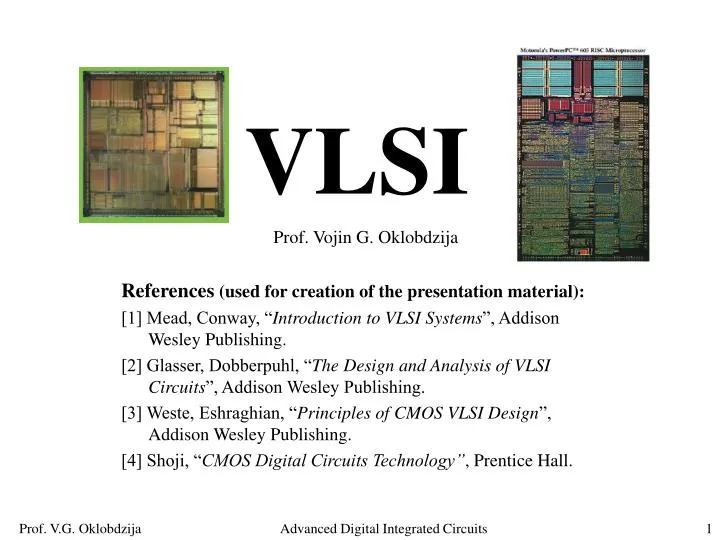
VLSI. Prof. Vojin G. Oklobdzija References (used for creation of the presentation material): [1] Mead, Conway, “ Introduction to VLSI Systems ”, Addison Wesley Publishing. [2] Glasser, Dobberpuhl, “ The Design and Analysis of VLSI Circuits ”, Addison Wesley Publishing.

E N D
VLSI Prof. Vojin G. Oklobdzija References (used for creation of the presentation material): [1] Mead, Conway, “Introduction to VLSI Systems”, Addison Wesley Publishing. [2] Glasser, Dobberpuhl, “The Design and Analysis of VLSI Circuits”, Addison Wesley Publishing. [3] Weste, Eshraghian, “Principles of CMOS VLSI Design”, Addison Wesley Publishing. [4] Shoji, “CMOS Digital Circuits Technology”, Prentice Hall. Advanced Digital Integrated Circuits
Historical Overview • nMOS era: 1970-85 • Pass-transistor design • Domino CMOS, 1982 • NORA • DCVSL • CPL, DPL • DCVS-PG • SRPL • LEAP • SOI-CMOS Advanced Digital Integrated Circuits
n-MOS Design Era LSI started with nMOS: • pass-transistor design experience: • Flourished at the beginning of the nMOS era (popularized by Mead-Conway book) • Allows high density layout and compact design style • Fast: outperforming gate based design • Low in power • Drawbacks: • Not compatible with existing design tools • Exhibiting testability and reliability problems Advanced Digital Integrated Circuits
Pass-Transistor Design Another way of looking at Karnaugh Map: AND function Advanced Digital Integrated Circuits
Pass-Transistor Design Two-variable function Advanced Digital Integrated Circuits
Pass-Transistor Design “Threshold Voltage Drop” problem: Advanced Digital Integrated Circuits
Pass-Transistor Design Solving the “Threshold Voltage Drop” problem in CMOS: Advanced Digital Integrated Circuits
Pass-Transistor Design Function Generator Advanced Digital Integrated Circuits
Pass-Transistor Design Full 1-bit Adder Advanced Digital Integrated Circuits
Pass-Transistor Design Compact ALU Example (IBM PC/RT) Circ. 1984 Advanced Digital Integrated Circuits
Pass-Transistor Design Compact ALU Example (IBM PC/RT) Advanced Digital Integrated Circuits
Using Pass-Transistor Design to Speed-up Addition Advanced Digital Integrated Circuits
Review of CMOS Prof. Vojin G. Oklobdzija Advanced Digital Integrated Circuits
CMOS Basics Advanced Digital Integrated Circuits
CMOS Basics Advanced Digital Integrated Circuits
CMOS Basics Advanced Digital Integrated Circuits
CMOS Basics A complex path example: Advanced Digital Integrated Circuits
CMOS Basics More complex blocks are realizable in CMOS Primitive gates: Advanced Digital Integrated Circuits
Muli-Input NOR function in CMOS is slow CMOS Deficiencies: Various remedies: Advanced Digital Integrated Circuits
CMOS Deficiencies and Remedies Advanced Digital Integrated Circuits
CMOS Deficiencies and Remedies Advanced Digital Integrated Circuits
CMOS Basic Inverter Transfer function: Logic voltage levels are VOH and VOL and VIL and VIH The inverter transfer function lie within the shaded region Advanced Digital Integrated Circuits
CMOS Basic: Inverter Characteristic Advanced Digital Integrated Circuits
CMOS Basic: Inverter Characteristic Advanced Digital Integrated Circuits
CMOS Basic: Inverter Characteristic Transistors during the transition Advanced Digital Integrated Circuits
CMOS Basic: Inverter Switching Advanced Digital Integrated Circuits
CMOS Basic: Power • During the static state there is no current • Current is only present during transistion: • Short circuit current (crow-bar current) • Charging and discharging of the output capacitor • Leakage Current Advanced Digital Integrated Circuits
CMOS Basic: Power This is an E=mc2 of low-power design There are three ways to control power: • Reducing Power-Supply Voltage (most effective !!) • Reducing the switching activity k (various ways) • Reducing CL (technology scaling etc.) • Reducing the required frequency of operation (?) PCMOS=kCLV2DDfo Advanced Digital Integrated Circuits
CMOS Basic: Delay • Which one of the three designs is the fastest ? • How can we find this out without simulation ? Learn about Logical Effort ! Advanced Digital Integrated Circuits
CMOS Basic: Delay Advanced Digital Integrated Circuits
CMOS Basic: Delay Delay can be approximated with: RND7Cin1+RNORCin2+RND2Cout Advanced Digital Integrated Circuits
CMOS Basic: Delay Delay of a signal path in CMOS logic is dependent on: • Fan-in of a gate • Represented as a resistance of the pull-up/down transistor path of the gate • Fan-out of a gate • Represented as a capacitive load at the output • Number of CMOS blocks in the path. • Wire delay connecting various blocks. Advanced Digital Integrated Circuits
CMOS Basic: Delay Delay of a signal path in CMOS logic can be reduced by: • Making the transistors larger in order to minimize resistance of a pull-up/down path in the gate • Making the transistors smaller in order to minimize the capacitive load of each gate • Reducing the number of CMOS blocks in the path. • Bringing the blocks closer and/or choosing the less wire intensive topology. • Note that these requirements are often contradictory Advanced Digital Integrated Circuits
CMOS Basic: Delay • How to estimate delay and critical timing in CMOS circuits ? • How to determine the proper transistor sizing in order to make a compromise with contradicting requirements ? • How to choose the right circuit topology ? The Answer: “Logical Effort” Advanced Digital Integrated Circuits