Download
1 / 12
120 likes | 199 Views
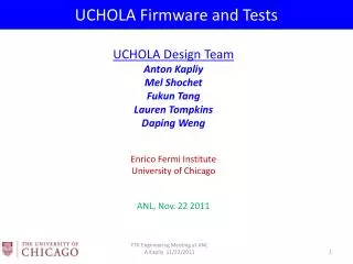
Dual-output hola FIRMWARE AND TESTS. Anton Kapliy Mel Shochet Fukun Tang Daping Weng. Summary. New dual-output HOLA board design with independent flow control from DAQ and FTK channels See Fukun Tang’s slides for a detailed walkthrough

E N D
Dual-output holaFIRMWARE AND TESTS Anton Kapliy Mel Shochet FukunTang DapingWeng
Summary • New dual-output HOLA board design with independent flow control from DAQ and FTK channels • See Fukun Tang’s slides for a detailed walkthrough • New firmware to interface the S-LINK core to inexpensive Altera Cyclone IV GX transceivers • 90% of original HOLA code preserved. • Fitting & assembling performed in Quartus 10.1 SP1 • We also have an experimental port to Quartus 11.0 (released in May 2011) • Simulation using a comprehensive Modelsim testbench • Manufactured, stuffed, and tested two prototype boards: • Firmware loaded on power-up from a 4 Mbit EPROM (EPCS4) • Data sent through both channels • Ensured that flow control can be asserted from either channel • BER tests using 1.35E15 bits sent through both channels
What is a HOLA? A device that implements the S-LINK protocol for point-to-point data transfer. Pixel and SCT data in a ROD is organized into 32-bit chunks and sent to a HOLA card, which serializes and sends it through optical fibers. Another HOLA card receives this data stream in a ROB (and FTK DF) and de-serializes it. S-LINK implements data framing, error detection, and flow-control.
Big picture: original HOLA LSC FPGA (only forward channel shown) Mezzanine data port D[32] @ 50 MHz D[32] @ 40 MHz FIFO Interface to TLK TX_EN TX_ER D[16] @ 100 MHz TLK2501 chip (sends data) • FPGA provides a parallel interface to an outside SERDES device (TLK-2501), which feeds serial signal to an optical transmitter. • However, TLK-2501: • Is deprecated and not marketed by TI anymore • Costs more than a Cyclone IV FPGA • Consumes four times as much power Serial connection (via optical transceiver) TLK2501 chip (receives data)
Big picture: new HOLA LSC FPGA (only forward channel shown) Mezzanine data port D[32] @ 50 MHz D[32] @ 40 MHz FIFO Interface to TLK TX_EN TX_ER OLD LSC CORE D[16] @ 100 MHz TX_CLK ALTGX wrapper (emulates TLK2501) (Altera SERDES megafunction) • 90% of original LSC code is unchanged. • ALTGX wrapper emulates TLK2501: • “Plugs in” into the original LSC core code • Implements link startup and synchronization • TLK receiver on DAQ side is oblivious to the change Serial connections (via optical transceivers) TLK2501 chip (DAQ) Xilinx FPGA (FTK DF)
Modelsim testbench ROD DAQ/FTK ROB • Stefan Haas gave us a Modelsim testbench implementing the above configuration. • We updated some features of this testbench to fit our purposes: • Serial LSC <-> LDC communication is simulated using Altera transceivers • LSC gains another channel (thus, “dual-output” HOLA) • Another LDC+ROMB block was added to receive data from the second channel. • FEMB, LDC, and ROMB were simulated functionally, while LSC (including Altera transceiver interface) - using a compiled & fitted (gate-level) Altera Quartus design.
PC setup: ROD side S32PCI64 “SOLAR” mezzanine card: Provides access to S-LINK via PCI bus The first prototype of dual-output HOLA 2 x optical transceivers Mezzanine connector to transfer 32-bit data S-LINK LSC FEMB
PC setup: ROB and FTK side Identical data is received from the two fibers running from the dual-output HOLA. Note that each channel can assert flow control. • “FILAR” card (based on S32PCI64): • Implements S-LINK protocol • Provides access to S-LINK via PCI bus FTK DAQ Multi-mode fibers Optical attenuators (7 db @ 850 nm)* The two channels are read out independently. E.g., we can read out all pending buffers from DAQ, so that only FTK will be asserting flow control. S-LINK LDC and ROMB (in one package) * We also ran BER tests to ~2E14 bits using attenuators rated for 10 db @ 1310 nm
BER test with 1.35E15 bits • We use the so-called SLIDAS mode in SOLAR PCI card • For the main BER test, we used the following configuration: • Continuous frames with 254 words x 32 bitsare fed into HOLA LSC • These words follow a pseudo-random sequence reproducible in C++ • On reception, we check word-by-word that all received patterns are correct • PC presents a bottleneck: need to generate these pseudo-random patterns and compare them with received data words. • We can achieve about 65 MB/s (21 days to test BER to 1E15). • Under this scheme, we continuously exercise flow control: • FEMB wants to send data at nearly 200 MB/s, but ROMB & LDC buffers quickly fill up and assert flow control until they are read out and “recharged” by the slow PC • Effectively, flow control is asserted / de-asserted continuously • 1.35E15 bits were received by both FILAR channels without any error (~4 weeks of non-stop transmission)
Additional tests • After the BER test was completed, Daping spent a couple of weeks running additional tests: • Generating data on the PC (rather than using SLIDAS patterns) • Send data to the SOLAR card via the first PCI port • Read it back on reception from the FILAR via the second PCI port. • SLIDAS random data with 16-1024 words per frame • Theoretically, the frames can be even larger, but our FILAR device drivers are hardcoded to allocate enough memory only for 1024 words. • ROD mode • Specially-designed frames that look like LHC data • Each frame contains a header, payload, and a footer • TEST mode (a walking-bit pattern) • All tests have finished without any errors
SLIDAS ROD mode A Typical Frame: Control word 3994170606 32 33685504 0 N (mark of the Nth frame) 3N-2 mod 4096 0 0 0 0 1 2 3 . . . Frame length – 15 1 Frame length – 14 0 Control word • Data pattern: • There is one control word at the beginning of each frame • Next is a header of length 9 words, containing information indicating that this is the Nth frame sending • The header is followed by an increasing arithmetic progression starting from 0 and ending at (frame length – 15) • Next is a footer of length 3 words • Ending control word • Length options are the same as in the random data mode • We tested to the order of 1E9 words, 256 words per frame and no error was observed