Download
1 / 12
120 likes | 260 Views
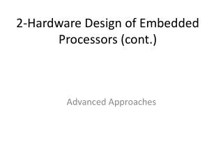
2-Hardware Design Basics of Embedded Processors (cont.). Outline. Introduction Combinational logic Sequential logic Custom single-purpose processor design RT-level custom single-purpose processor design. …. …. external control inputs. external data inputs. controller. datapath.

E N D
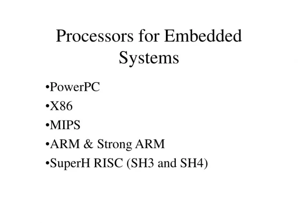
Outline • Introduction • Combinational logic • Sequential logic • Custom single-purpose processor design • RT-level custom single-purpose processor design
… … external control inputs external data inputs controller datapath … … registers datapath control inputs next-state and control logic controller datapath datapath control outputs functional units state register … … external control outputs external data outputs … … a view inside the controller and datapath controller and datapath Custom single-purpose processor basic model
!1 1: (a) black-box view 1 !(!go_i) 2: !go_i x_i GCD go_i y_i 2-J: 3: x = x_i d_o 4: y = y_i !(x!=y) 5: x!=y 6: x<y !(x<y) y = y -x x = x - y 7: 8: 6-J: 5-J: d_o = x 9: 1-J: Example: greatest common divisor • First create algorithm • Convert algorithm to “complex” state machine • Known as FSMD: finite-state machine with datapath • Can use templates to perform such conversion (c) state diagram (b) desired functionality 0: int x, y; 1: while (1) { 2: while (!go_i); 3: x = x_i; 4: y = y_i; 5: while (x != y) { 6: if (x < y) 7: y = y - x; else 8: x = x - y; } 9: d_o = x; }
Assignment statement Loop statement Branch statement a = b next statement while (cond) { loop-body- statements } next statement if (c1) c1 stmts else if c2 c2 stmts else other stmts next statement !cond a = b C: C: c1 !c1*!c2 !c1*c2 cond next statement c1 stmts c2 stmts others loop-body- statements J: J: next statement next statement State diagram templates
!1 1: 1 !(!go_i) 2: x_i y_i !go_i Datapath 2-J: x_sel n-bit 2x1 n-bit 2x1 3: x = x_i y_sel x_ld 0: x 0: y 4: y = y_i y_ld !(x!=y) 5: != < subtractor subtractor x!=y 5: x!=y 5: x!=y 6: x<y 8: x-y 7: y-x 6: x_neq_y x<y !(x<y) x_lt_y 9: d y = y -x x = x - y 7: 8: d_ld d_o 6-J: 5-J: d_o = x 9: 1-J: Creating the datapath • Create a register for any declared variable • Create a functional unit for each arithmetic operation • Connect the ports, registers and functional units • Based on reads and writes • Use multiplexors for multiple sources • Create unique identifier • for each datapath component control input and output
!1 go_i 1: Controller !1 1 !(!go_i) 1: 0000 2: 1 !(!go_i) 0001 2: x_i y_i !go_i !go_i Datapath 2-J: 0010 2-J: x_sel n-bit 2x1 n-bit 2x1 3: x = x_i x_sel = 0 x_ld = 1 0011 3: y_sel x_ld 0: x 0: y 4: y = y_i y_sel = 0 y_ld = 1 y_ld 0100 4: !(x!=y) 5: !x_neq_y 0101 5: != < subtractor subtractor x!=y x_neq_y 5: x!=y 5: x!=y 6: x<y 8: x-y 7: y-x 6: 0110 6: x_neq_y x<y !(x<y) x_lt_y !x_lt_y x_lt_y 9: d y = y -x x = x - y y_sel = 1 y_ld = 1 x_sel = 1 x_ld = 1 7: 8: 7: 8: d_ld 0111 1000 d_o 6-J: 1001 6-J: 5-J: 1010 5-J: d_o = x 9: d_ld = 1 1011 9: 1-J: 1100 1-J: Creating the controller’s FSM • Same structure as FSMD • Replace complex actions/conditions with datapath configurations
x_i y_i (b) Datapath x_sel n-bit 2x1 n-bit 2x1 y_sel x_ld 0: x 0: y y_ld != < subtractor subtractor Controller implementation model 5: x!=y 5: x!=y 6: x<y 8: x-y 7: y-x go_i x_neq_y x_sel Combinational logic y_sel x_lt_y 9: d x_ld d_ld y_ld d_o x_neq_y x_lt_y d_ld Q3 Q2 Q1 Q0 State register I3 I2 I1 I0 Splitting into a controller and datapath go_i Controller !1 1: 0000 1 !(!go_i) 0001 2: !go_i 0010 2-J: x_sel = 0 x_ld = 1 0011 3: y_sel = 0 y_ld = 1 0100 4: x_neq_y=0 0101 5: x_neq_y=1 0110 6: x_lt_y=1 x_lt_y=0 y_sel = 1 y_ld = 1 x_sel = 1 x_ld = 1 7: 8: 0111 1000 1001 6-J: 1010 5-J: d_ld = 1 1011 9: 1100 1-J:
Inputs Outputs Q3 Q2 Q1 Q0 x_neq_y x_lt_y go_i I3 I2 I1 I0 x_sel y_sel x_ld y_ld d_ld 0 0 0 0 * * * 0 0 0 1 X X 0 0 0 0 0 0 1 * * 0 0 0 1 0 X X 0 0 0 0 0 0 1 * * 1 0 0 1 1 X X 0 0 0 0 0 1 0 * * * 0 0 0 1 X X 0 0 0 0 0 1 1 * * * 0 1 0 0 0 X 1 0 0 0 1 0 0 * * * 0 1 0 1 X 0 0 1 0 0 1 0 1 0 * * 1 0 1 1 X X 0 0 0 0 1 0 1 1 * * 0 1 1 0 X X 0 0 0 0 1 1 0 * 0 * 1 0 0 0 X X 0 0 0 0 1 1 0 * 1 * 0 1 1 1 X X 0 0 0 0 1 1 1 * * * 1 0 0 1 X 1 0 1 0 1 0 0 0 * * * 1 0 0 1 1 X 1 0 0 1 0 0 1 * * * 1 0 1 0 X X 0 0 0 1 0 1 0 * * * 0 1 0 1 X X 0 0 0 1 0 1 1 * * * 1 1 0 0 X X 0 0 1 1 1 0 0 * * * 0 0 0 0 X X 0 0 0 1 1 0 1 * * * 0 0 0 0 X X 0 0 0 1 1 1 0 * * * 0 0 0 0 X X 0 0 0 1 1 1 1 * * * 0 0 0 0 X X 0 0 0 Controller state table for the GCD example
… … controller datapath registers next-state and control logic functional units state register … … a view inside the controller and datapath Completing the GCD custom single-purpose processor design • We finished the datapath • We have a state table for the next state and control logic • All that’s left is combinational logic design • This is not an optimized design, but we see the basic steps
Sender Bridge A single-purpose processor that converts two 4-bit inputs, arriving one at a time over data_in along with a rdy_in pulse, into one 8-bit output on data_out along with a rdy_out pulse. Receiver rdy_in rdy_out Problem Specification clock data_in(4) data_out(8) Bridge rdy_in=0 rdy_in=1 rdy_in=1 WaitFirst4 RecFirst4Start data_lo=data_in RecFirst4End rdy_in=0 rdy_in=0 rdy_in=1 rdy_in=1 WaitSecond4 RecSecond4Start data_hi=data_in RecSecond4End FSMD rdy_in=0 Inputs rdy_in: bit; data_in: bit[4]; Outputs rdy_out: bit; data_out:bit[8] Variables data_lo, data_hi: bit[4]; Send8Start data_out=data_hi & data_lo rdy_out=1 Send8End rdy_out=0 RT-level custom single-purpose processor design • We often start with a state machine • Rather than algorithm • Cycle timing often too central to functionality • Example • Bus bridge that converts 4-bit bus to 8-bit bus • Start with FSMD • Known as register-transfer (RT) level • Exercise: complete the design
rdy_in=0 rdy_in=1 rdy_in=1 WaitFirst4 RecFirst4Start data_lo_ld=1 RecFirst4End rdy_in=0 rdy_in=0 rdy_in=1 rdy_in=1 WaitSecond4 RecSecond4Start data_hi_ld=1 RecSecond4End Send8Start data_out_ld=1 rdy_out=1 Send8End rdy_out=0 RT-level custom single-purpose processor design (cont’) Bridge (a) Controller rdy_in rdy_out clk data_in(4) data_out data_hi data_lo to all registers data_lo_ld data_hi_ld data_out_ld data_out (b) Datapath