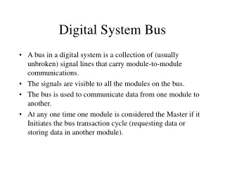
Download
1 / 10
100 likes | 252 Views
Dorothy Gordon. Digital Sub-System. Overview. Digital Subsystem Overview/Block Diagram Developments Since PDR Design/Implementation Status Next. 27 June 2006. Digital Engineering. 2. Digital Sub-System Data Flow. 27 June 2006. Digital Engineering. 3. Digital Sub-System Block Diagram.

E N D
Dorothy Gordon Digital Sub-System
Overview • Digital Subsystem Overview/Block Diagram • Developments Since PDR • Design/Implementation Status • Next 27 June 2006 Digital Engineering 2
Digital Sub-System Data Flow 27 June 2006 Digital Engineering 3
Developments since PDR • Requirements – no significant changes • Parts Selection • DDC BU-63705 for 1553 Bus, Actel SX72, Amptek PH300 • DC-DC Converter Modules (International Rectifier) • Peak Stretcher (PH300): Performance Verified via Breadboard • Functional Description/Specification • Details of FPGA operation (Drawing # 32-03010) • Schematics • Board Schematics: released (Drawing # 32-03003) • Chassis Schematics: released (Drawing # 32-03006) • High Voltage Power Supply (Drawing #32-03003.01) • (subcontracted) design complete – prototype in house 27 June 2006 Digital Engineering 5
Since PDR (continued) • Peer Review (GSFC, May 22, 2006) • Received/Answered 15 RFAs (for both analog and digital subsystems) • No change to fundamental design of either subsystem • Part type modification (to insure edge-rate compatibility) • Actel Programming Socket exchanged (for “ESD Friendly” replacement) • Actel Static Timing analysis to include asynchronous clocked path analysis • Signal Integrity and Ground bounce concerns (especially relative to the SX72 FPGA) • Analysis • Parts Stress Analysis: released (Drawing #32-03010.03) • Worst Case Analysis: released (Drawing #32-04011.02)
Design/Implementation Status • FPGA Design • VHDL Coding Complete (Drawing #32-03003.10) • Top Level functional simulation complete • Timing Verified (Static Timer and Dynamic Simulation) • Engineering Board (ETU) Layout and Fabrication completed • Engineering layout is flight part footprint compatible • High Voltage Supply, implemented on hand-wired breadboard, will be integrated during the second layout stage • ETU Population • Completion expected by last week of June 27 June 2006 Digital Engineering 7
Next • Design Complete – ready for board level check-out • Next • Test with GSE • Verify basic functionality/operation • Develop/run marathon diagnostics • Integrate with analog board • Flight Version • Incorporate any modifications resulting from ETU debug • Add Bias (High Voltage) Supply