Download
1 / 22
220 likes | 354 Views
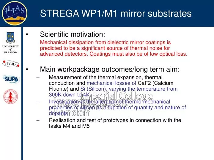
STREGA WP1/M1 mirror substrates. Scientific motivation: Mechanical dissipation from dielectric mirror coatings is predicted to be a significant source of thermal noise for advanced detectors. Coatings must also be of low optical loss. Main workpackage outcomes/long term aim:

E N D
STREGA WP1/M1 mirror substrates • Scientific motivation: Mechanical dissipation from dielectric mirror coatings is predicted to be a significant source of thermal noise for advanced detectors. Coatings must also be of low optical loss. • Main workpackage outcomes/long term aim: • Measurement of the thermal expansion, thermal conduction and mechanical losses of CaF2 (Calcium Fluorite) and Si (Silicon), varying the temperature from 300K down to 4K. • Investigation of the alteration of thermo-mechanical properties of silicon as a function of quantity and nature of dopants • Realisation and test of prototypes in connection with the tasks M4 and M5 • GEO • LIGO • ISA
Status at last meeting Clamp • Preliminary room T measurements of mechanical dissipation of two silicon samples of identical geometry, supplied by Stanford, was measured over a range of frequencies. Suspension thread/wire Test mass To high voltage Excitation plate (behind mass) Schematic diagram of front view of suspended test mass. Silicon samples cut along different crystal axes, [111] and [100]. The [111] sample was boron-doped.
Status at last meeting Measured loss factors for two samples of bulk silicon Sample [b] typically showed lower dissipation Sample [a]: [100] cut, nominally undoped Sample [b]: [111] cut, boron doped Reason for difference seen in measured loss factors (eg crystalline orientation, dopant, other?) is under investigation Some evidence to suggest may be due to crystalline orientation • Lowest loss obtained so far = (9.6±0.3)10-9 • Comparable with the lowest loss factors measured at room temperature [a] [b]
Consider the [100] sample Q of two modes of the sample studied as a function of orientation of sample in suspension loop FE model of relative displacement of surface for 2 modes of sample Friction at suspension points is clearly significant and dependent on position of crystal Mode shapes are dependent on crystal axis
Future plans • Constructing a prototype ‘nodal support’ system to attempt to reduce suspension losses for these samples • Several sets of samples purchased of various aspect ratios and different crystal cuts for further study • Measurements of bulk silicon at cryogenic temperature • Second cryostat being commissioned in Glasgow • Sample suspended – initial cooling taking place this week
STREGA WP1/M5 suspension substrates • Suspension technology status: • To achieve the desired sensitivities of future long-baseline gravitational wave detectors will require a reduction in thermal noise associated with test masses and their suspensions • Requirement to develop ultra-low thermal noise suspensions for 3rd generation detections (cryogenic temperatures) Future eg. EGO Advanced eg. AdLIGO Current eg. GEO600 Silicon suspension technology
Silicon cantilever fabrication • Initial samples have been fabricated by etching from silicon wafers at Stanford (Stefan Zappe) Set of samples fabricated with varying properties and dimensions: • 1 x 10⁻³ Ohm-cm to >100 Ohm-cm • ~40 microns to ~100’s mm thick • First sample studied: • P-type doping (Boron), resistivity = 10-20 Ohm-cm • ~ 92 microns thick • Resonant modes of samples excited using an electrostatic drive • Sample displacement monitored using shadow sensor • Measure rate of decay of the mode amplitudes, from which mechanical dissipation, f(w0) can be determined.
Experimental setup • GEO • LIGO • ISA
The two cantilevers tested • GEO Identical material properties. • LIGO • ISA Thermoelastic curves for tested cantilevers with marked cantilever resonant frequencies
Experimental measurements • Measured dissipation is the sum of dissipation arising from a number of sources: measurements in vacuum <10-5 Torr rigid clamp holding thick end of sample calculate from silicon material properties measurements of samples of varying surface to volume ratios should allow estimates
Temperature dependence of (a) measured loss, and (b) calculated thermoelastic loss for bending mode at 670Hz (cant length 57mm) 4.7x10⁻⁷
Temperature dependence of (a) measured loss, and (b) calculated thermoelastic loss for bending mode at 2185Hz. (cant length 57mm)
Temperature dependence of (a) measured loss, and (b) calculated thermoelastic loss for bending mode at 1935Hz. (cant length 34mm)
Temperature dependence of (a) measured loss, and (b) calculated thermoelastic loss for bending modes at 3785 Hz and 6265 Hz. (cant l = 34mm)
Results and interpretation • The intermittent dissipation peaks observed appear related to changes in temperature distribution in system • Suggests they are due to energy coupling to resonances in the clamping structure • Also need to consider surface effects (sample is 92 microns thick)
Surface losses • Yasumura et al. measured the loss factors of single-crystal cantilevers with thickness 0.06 0.24 mm and found they could be represented by: • fsurface is the limit to the measurable loss of a cantilever of thickness t and Young’s modulus E1 set by the presence of a surface layer of: • Surface layer thickness d, • Young’s modulus E1S, and • loss fs • For simplicity assume, E1E1S • Can use the above to estimate limit to measurable loss for our sample set by surface loss
Ave. loss of third bending mode (670Hz) compared to • (b) sum of scaled surface loss + calculated th-elas loss. Surface effects are significant but do not account for total loss measured - next source to investigate is ‘stick-slip’ damping of end of sample in clamp
Results and interpretation • Studies have been carried out to investigate energy coupling to the clamping structure
Normalised piezo response showing energy coupling from resonating cantilever into steel clamp at 1.3, 2.2 and 3.1 kHz
Response of the clamping structure to a constant driving signal from 2-3 kHz at 240, 270 and 285 K from 2–3 kHz.
The measured dissipation Q-1 in silicon oscillators (kHz frequency band) 1 – Calculated from “phonon-phonon” mechanism(f = 10 kHz) 2 – MSU – 1980, unpublished (t 10 cm, f = 10 kHz) 3 – D.F. McGuigan et al., J.Low Temp.Phys. 30 (1978), 621 (t 10 cm, f = 19.5 kHz) 4 – B.H.Houston et al., Appl.Phys.Lett. 80 (2002), 1300 (t 100 m, f = 5.5 kHz) 5 – U.Gysin et al., Phys.Rev. B69 (2004), 045403(t 2 m, f = 10.8 kHz) Slide courtesy of V. Mitrofanov, Moscow State University
Summarise • So far we do not see evidence of dissipation peaks intrinsic to our sample • Evidence of coupling to resonances of clamping structure under investigation In short term: • We will study both thinner and thicker samples to further quantify surface loss effects • Reduce surface loss effects to allow studies of other dissipation mechanisms presents In medium term: • Continue studies of effects of doping on intrinsic dissipation and thermoelastic loss