Download
1 / 33
330 likes | 579 Views
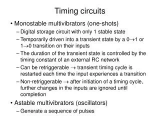
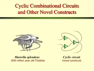
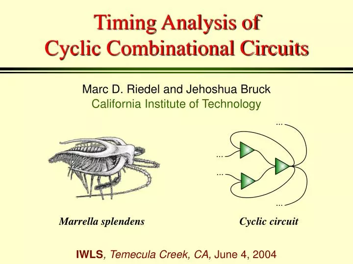
Timing Analysis of Cyclic Combinational Circuits. Marc D. Riedel and Jehoshua Bruck. California Institute of Technology. Marrella splendens. Cyclic circuit. IWLS , Temecula Creek, CA, June 4, 2004. inputs. outputs. combinational logic. Combinational Circuits.

E N D
Timing Analysis of Cyclic Combinational Circuits Marc D. Riedel and Jehoshua Bruck California Institute of Technology Marrella splendens Cyclic circuit IWLS, Temecula Creek, CA, June 4, 2004
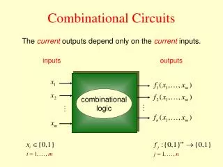
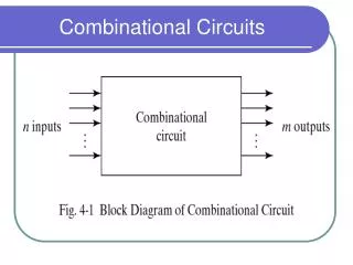
inputs outputs combinational logic Combinational Circuits The current outputsdepend only on the current inputs.
x c y AND z OR x AND z y XOR s XOR Combinational Circuits Generally acyclic (i.e., feed-forward) structures.
Circuit is cyclic yet combinational; computes functions and with 6 gates. AND OR AND OR AND OR Cyclic Combinational Circuits An acyclic circuit computing these functions requires 8 gates. x a b x c d
x c y g1 z g4 x g3 z y g2 s g5 level: Timing Analysis Predicated on a topological ordering. l1= 1 l4= 3 l3= 2 l2= 1 l5= 2
arrival times level: Timing Analysis Predicated on a topological ordering. l1= 1 10 l4= 3 x 11 12 c l3= 2 10 y g1 10 z g4 02 l2= 1 10 x g3 l5= 2 z 10 01 10 y g2 s 12 g5 (assume a delay bound of 1 time unit for each gate)
Cyclic Combinational Circuits No topological ordering. x How can we perform timing analysis? AND a OR b AND x OR c AND d OR
Cyclic Combinational Circuits No topological ordering. 14 10 x How can we perform timing analysis? AND 15 00 a OR 16 10 b AND 11 10 x OR 12 10 c AND 13 00 d OR
Prior Work In previous papers, we presented: • Algorithms for functionalanalysis(IWLS’03); • Strategies for synthesis (DAC’03). In trials on benchmark circuits, cyclic optimizations reduced the area of by as much as 30%
Optimization for Area application of “script.rugged” and mapping Number of NAND2/NOR2 gatesin Berkeley SIS vs.CYCLIFYsolutions
Contributions In this paper, we discuss: • An algorithm for timing analysis. • Synthesis results, with optimization jointly targetingarea and delay. In trials on benchmarks circuits, cyclic optimizations simultaneously reduced the area by up to 10% and thedelay by up to 25%.
minimum-cutfeedback set inputs outputs Related Work Malik (1994), Hsu, Sun and Du (1998), and Edwards (2003) considered analysis techniques for cyclic circuits. Their approach: identify equivalent acyclic circuits. acyclic circuit cyclic circuit Unravelling cyclic circuits this way is a difficult task.
inputs outputs cyclic circuit Our Approach Perform event propagation, directly on a cyclic circuit. 10 00 16 10 13 10 00
Our Approach Perform event propagation, directly on a cyclic circuit. Compute events symbolically, with BDDs. [x]0 [a]0 f1=[b(a+x(c+d))]6 cyclic circuit [b]0 f2=[d+c(x+ba))]6 [c]0 [d]0
all wires are assumed to have unknown/undefined values ( ). • the primary inputs assume definite values in {0, 1}. Circuit Model Perform static analysis in the “floating-mode”. At the outset: a “controlling” input full set of“non-controlling” inputs unknown/undefinedoutput
all wires are assumed to have unknown/undefined values ( ). • the primary inputs assume definite values in {0, 1}. ^ ^ ^ ^ ^ 1 AND OR Circuit Model Perform static analysis in the “floating-mode”. At the outset: During the analysis, only signals driven(directly or indirectly)by the primary inputs are assigned definite values.
AND Circuit Model Up-bounded inertial delay model. Ensuresmonotone speed-up property. each gate has delay in [0, td]
AND Circuit Model The arrival time at a gate output is determined: • either by the earliestcontrollinginput. 02 13 03 06 (assuming a delay bound of 1)
AND Circuit Model The arrival time at a gate output is determined: • either by the earliestcontrollinginput; • or by the latestnon-controllinginput. 12 13 17 16 (assuming a delay bound of 1)
set of input assignments for which output is Timing Analysis Characterize arrival times symbolically (with BDDs): : set of input assignments that produce 0 : set of input assignments that produce 1 Implicitly:
arrival time Timing Analysis Characterize arrival times symbolically (with BDDs): : set of input assignments that produce 0 : set of input assignments that produce 1 Time-stamp the characteristic sets:
Initialization internal signals: primary inputs: x
Propagation If there is a change in the characteristic set of a gate’s fan-in: For a controlling input value v, producing an output value w,
Propagation If there is a change in the characteristic set of a gate’s fan-in: For non-controlling input values v1, v2,v3 producing an output value w,
If changes as a result, update its time-stamp: Propagation If there is a change in the characteristic set of a gate’s fan-in: delay in [0, td]
0 Example time 3 time 6 time 5 time 4 time 1 time 2 0 AND 0 x OR 0 0 a AND 0 b 0 OR 0 x 0 AND 0 c OR 0 0 d
The algorithm terminates since the cardinality of each set increases over time; at most . • The circuit is combinational iff the “care” set of input assignments is contained within for each output gate gi . • The delay bounds on the arrival times for the output gates give a boundon the circuit delay. Timing Analysis
Multi-Terminal BDDs For finer-grained timing information,preserve a history of the changes. Reference: Bahar et al., “Timing Analysis using ADDs"
Synthesis N1 N3 N2 Select best solution through a branch-and-bound search. N4 N6 Analysis algorithm is used to validate and rank potential solutions. N5 N7 N9 N8 See The Synthesis of Cyclic Combinational Circuits,DAC’03.
Implementation: CYCLIFY Program • Incorporated synthesis methodology in a general logic synthesis environment (Berkeley SIS package). • Trials on wide range of circuits • randomly generated • benchmarks • industrial designs. • Conclusion: nearly all circuits of practical interest can be optimized with feedback.
Optimization for Area and Delay application of “script.delay” and mapping Area and Delay of Berkeley SIS vs.CYCLIFYsolutions. Area: number of NAND2/NOR2 gates. Delay:1 time unit/gate.
Discussion • Nearly all circuits can be optimized with cycles. • Optimizations are significant. Analysis throughsymbolic event propagation: • Existing methods can be applied to cyclic circuits. • Complexity is comparable for cyclic and acyclic circuits. Synthesis strategies targeting area and delay:
Future Directions • Apply more realistic timing models for analysis. • Use more efficient symbolic techniques (e.g., use boolean satisfiability (SAT)-based techniques). • Incorporate more sophisticated search heuristics into synthesis.